3 major misunderstandings of differential signal PCB layout, do not regret
[Guide] The most important rule in the design of PCB differential traces is the matching line length. Other rules can be flexibly processed according to design requirements and practical applications. At the same time, in order to compensate for the impedance matching, a matching resistor can be added between the differential pair of the receiving end. Its value should be equal to the value of the differential impedance. This signal quality will be better.
Misunderstanding one
It is considered that the differential signal does not require a ground plane as a return path, or that the differential traces provide a return path to each other. The cause of this misunderstanding is that it is confused by surface phenomena, or the understanding of the mechanism of high-speed signal transmission is not deep enough. Although the differential circuit is insensitive to similar ground bounce and other noise signals that may be present on the power and ground planes. The partial return cancellation of the ground plane does not mean that the differential circuit does not use the reference plane as the signal return path. In fact, in the signal reflow analysis, the mechanism of the differential trace is the same as that of the ordinary single-ended trace, that is, the high frequency signal is always The reflow is performed along the loop with the smallest inductance. The biggest difference is that in addition to the coupling to the ground, the differential lines have mutual coupling, and which one is strong, which becomes the main return path.
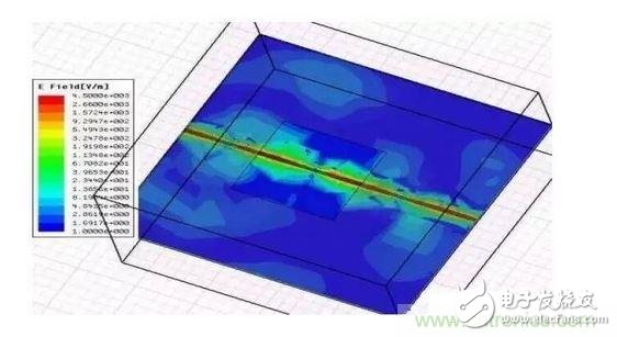
In the PCB circuit design, the coupling between the differential traces is generally small, often only 10 to 20% of the coupling degree, and more is the coupling to the ground, so the main return path of the differential traces still exists in the ground plane. . When the local plane is discontinuous, there is no reference plane, and the coupling between the differential traces provides the main return path. Although the discontinuity of the reference plane does not have a serious effect on the differential traces, it will reduce the quality of the differential signals and increase the EMI, which should be avoided. Some designers believe that the reference plane below the differential trace can be removed to suppress some of the common-mode signals in the differential transmission, but in theory this approach is not advisable. How is the impedance controlled? Not providing the ground impedance loop to the common mode signal will inevitably cause EMI radiation, which is more harmful than good.
So keep the PCB ground plane return path wide and short. Try not to cross the island (crossing the adjacent power supply or the separation area of ​​the ground.) For example, USB and SATA and PCI-EXPRESS in the motherboard design, it is best not to have an inter-island approach. Ensure that the underside of these signals is a complete ground plane or power plane.
Misunderstanding 2
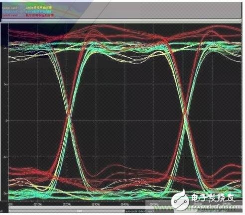
It is considered more important to keep the equal spacing longer than the matching line length. In actual PCB layout, the requirements of differential design cannot often be met at the same time. Due to factors such as pin distribution, vias, and routing space, the wire length matching must be achieved by proper winding, but the result is necessarily that the partial regions of the differential pair cannot be parallel, but the spacing is not equal. The impact is minimal, and in comparison, line length mismatch has a much greater impact on timing. From the theoretical analysis, although the inconsistency of the spacing will cause the differential impedance to change, but because the coupling between the differential pairs is not significant, the range of impedance variation is also very small, usually within 10%, only equivalent to one The reflection caused by the hole, which does not have a significant effect on the signal transmission. Once the line length is not matched, in addition to the offset in the timing, the common mode component is introduced into the differential signal, which reduces the signal quality and increases EMI.
It can be said that the most important rule in the design of PCB differential traces is the matching line length. Other rules can be flexibly processed according to design requirements and practical applications. At the same time, in order to compensate for the impedance matching, a matching resistor can be added between the differential pair of the receiving end. Its value should be equal to the value of the differential impedance. This signal quality will be better.
Therefore, the following two points are suggested:
Use the terminating resistor to achieve the maximum matching of the differential transmission line. The resistance is generally between 90 and 130 Ω. The system also needs this terminating resistor to generate the differential voltage for normal operation.
It is best to use a surface resistance of 1 to 2% accuracy across the differential line. If necessary, use two resistors with a resistance of 50Ω each, and ground the capacitor through a capacitor in the middle to filter out common mode noise.
Generally, the matching requirement for the equal-length CLOCK of the differential signal is within +/- 10 mils.
Misunderstanding three
Think that the differential traces must be close. Bringing the differential traces closer is nothing more than enhancing their coupling, both to improve immunity to noise and to take advantage of the opposite polarity of the magnetic field to counteract electromagnetic interference to the outside world. Although this practice is very beneficial in most cases, it is not absolute. If we can guarantee that they are fully shielded from external interference, then we do not need to let the strong coupling through each other to achieve anti-interference. And the purpose of suppressing EMI. How can we ensure that the differential traces have good isolation and shielding? Increasing the distance from other signal traces is one of the most basic ways. The electromagnetic field energy decreases with the square of the distance. When the line spacing is more than 4 times the line width, the interference between them is extremely weak. Can be ignored. In addition, the ground plane isolation can also be used for good shielding. This structure is often used in high-frequency (10G or more) IC package PCB design. It is called CPW structure and can guarantee strict differential impedance. Control (2Z0).
Differential traces can also be used in different signal layers, but this method is generally not recommended because differences in impedance, vias generated by different layers can disrupt the effects of differential mode transmission and introduce common mode noise. In addition, if the adjacent two layers are not tightly coupled, the ability of the differential traces to resist noise is reduced, but crosstalk is not an issue if the proper spacing from the surrounding traces is maintained. At normal frequencies (below GHz), EMI is not a serious problem. Experiments show that the differential energy of 500Mils is 60dB away from the radiated energy of 3m, which is enough to meet the FCC electromagnetic radiation standard. The designer does not have to worry too much about the electromagnetic incompatibility caused by insufficient coupling of the differential lines.
RF Cable, also known as Radio Frequency Cable, is a sophisticated coaxial cable tailored to efficiently propagate radio frequency signals across vast distances, ensuring minimal attenuation and signal loss. Its universal appeal stems from its inherent ability to shield against electromagnetic interference, maintain a stable impedance across its length, and support blazing-fast data transmission rates. As a cornerstone of diverse communication systems, RF Cable ensures a seamless flow of information from one end to the other, making it an indispensable component in today's interconnected world.
These cables are constructed with a central conductor, surrounded by an insulating material, a braided or foil shield, and an outer jacket. This unique structure provides both electrical and mechanical protection, allowing RF Cables to withstand harsh environments and maintain signal integrity. The central conductor carries the signal, while the shield effectively blocks external interference, enhancing signal quality.
RF Cables are available in a wide range of types, each tailored to specific applications and frequency ranges. From lightweight, flexible cables suitable for indoor use to rugged, outdoor-rated cables capable of enduring extreme weather conditions, the variety ensures that there's an RF Cable solution for every need.
Their applications span numerous industries, including telecommunications, broadcasting, military and aerospace, industrial automation, and testing and measurement. In telecommunications, RF Cables connect base stations to antennas, enabling wireless communication networks. In broadcasting, they transmit video and audio signals from studios to transmission towers. In the military and aerospace sectors, RF Cables are critical for secure, high-speed data links between aircraft, ships, and ground stations.
Overall, RF Cables are an indispensable element in modern communication systems, ensuring reliable and efficient signal transmission across diverse environments and applications.
RG58,LMR400,LMR200,Coaxial Cable,RF Cable,RG6,RG6 Coaxial Cable
Yetnorson Antenna Co., Ltd. , https://www.yetnorson.com