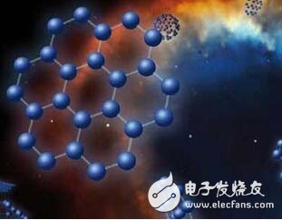
Detailed explanation of several mainstream production methods of graphene
There are several different methods for different materials and uses. Generally speaking, there are a vapor deposition method, a redox method, and an intercalation method.
The meteorological deposition method is mainly carbon-containing gas (methane, faint). Under certain temperature and pressure conditions, carbon atoms adhere to the growth base to form a single-layer carbon structure material and gradually grow.
Advantages: The obtained graphene structure is good and the size is not limited by the raw materials. Disadvantages: The preparation process is complicated and the production efficiency is low.
In the redox method, graphite is oxidized layer by layer using an oxidizing agent, and the oxidized layer is peeled off by ultrasonic or the like. Thereafter, the graphite oxide layer is reduced by a reducing agent to obtain graphene.

Advantages: low cost and high production efficiency.
Disadvantages: The size of the graphene produced is determined by the raw materials, and the oxidizing agent and reducing agent used may pollute the environment.
The intercalation method is to fill the intercalation material into the layer gap of the graphite, thereby overcoming the interlayer van der Waals force, so that the layers are dispersed, thereby obtaining graphene. This method is still in the research and development stage.
Micromechanical stripping
Graphene is first produced by micromechanical stripping. The micro-mechanical stripping method is to press the highly oriented pyrolytic graphite sheet onto other surfaces with a transparent tape to perform multiple peeling, and finally obtain a single layer or several layers of graphene. In 2004, Geim, Novoselov, etc. obtained the first single layer of graphene in the world by this method, which proved that the two-dimensional crystal structure can exist at normal temperature.
The micro-mechanical stripping method is simple in operation and high in sample quality, and is currently the main method for preparing single-layer high-quality graphene. However, its controllability is poor, and the produced graphene is small in size and has great uncertainty, while being low in efficiency and high in cost, and is not suitable for mass production.
Epitaxial growth method
The epitaxial growth method includes a silicon carbide epitaxial growth method and a metal catalytic epitaxial growth method. The silicon carbide epitaxial growth method refers to heating a SiC single crystal at a high temperature so that Si atoms on the surface of the SiC are evaporated to escape from the surface, and the remaining C atoms are reconstructed by an independent form to obtain graphene based on the SiC substrate.
The metal-catalyzed epitaxial growth method is to introduce a hydrocarbon into a catalytically active transition metal substrate such as Pt, Ir, Ru, Cu, etc. under ultra-high vacuum conditions, and catalytically dehydrogenate the adsorbed gas by heating to obtain graphene. . The gas can grow over the entire metal substrate during the adsorption process, and the growth process is a self-limiting process, that is, the substrate does not repeatedly absorb after adsorbing the gas. Therefore, the prepared graphene is mostly a single layer, and can be widely used. Uniform graphene was prepared.
Chemical vapor deposition CVD: the most promising large-scale production method
The CVD method is considered to be the most promising preparation of high-quality, large-area graphene, and is the most promising method for industrial production of graphene films. The specific process of the chemical vapor deposition CVD method is: introducing hydrocarbon methane, ethanol, etc. into the surface of the high-temperature heated metal substrate Cu, Ni, and cooling after a certain period of time, and several layers are formed on the surface of the substrate during the cooling process or Single-layer graphene, in which carbon atoms are dissolved and diffused on the substrate. The method is similar to the metal catalytic epitaxial growth method, and has the advantages that it can be carried out at a lower temperature, thereby reducing the energy consumption in the preparation process, and the graphene and the substrate can be easily separated by the chemical corrosion metal method, which is advantageous for The graphene is processed later.
Existing methods cannot meet the requirements of graphene industrialization. Numerous preparation methods including micro mechanical peeling, epitaxial growth, chemical vapor deposition CVD and graphite oxide reduction are still unable to meet the requirements of industrialization. In particular, industrialization requires graphene preparation technology to produce graphene with large area and high purity at a stable and low cost. This technical problem has not yet been solved.
Other methods for preparing graphene include a carbon nanotube cutting method, a graphite intercalation method, an ion implantation method, a high temperature and high pressure HPHT growth method, an explosion method, and an organic synthesis method.
The preparation of large-area, high-quality graphene remains a major challenge. Although chemical vapor deposition and redox processes can produce graphene in large quantities, chemical vapor deposition is more complicated in the later stage of preparation, and the process of graphene transfer is more complicated, and the preparation cost is higher. defect. When using the redox method, since the single-layer graphene is very thin and easy to agglomerate, the conductive property and specific surface area of ​​the graphene are lowered, which further affects the application in the photovoltaic device, and in addition, the graphene is easily caused in the redox process. Crystal structure defects, such as the loss of carbon atoms on the carbon ring.
The system restricts the industrialization of graphene. The various top properties of graphene can only be manifested when the quality of graphene is very high. As the number of layers increases and the accumulation of internal defects, the superior performance of graphene will be reduced. In order to truly realize the industrialization of graphene applications and reflect the superior quality of graphene in replacing other materials, it is necessary to seek breakthroughs in the preparation methods. Only the method of graphene suitable for industrialization has emerged, and the industrialization of graphene can really come.
Future Bus connectors Description
Future Bus connectors, which use 2mm style have a mating distance of 10mm. Both Future bus and the upgrade Future bus+ are out-dated.No additional work has been done to upgrade the specification over the years. However we still produce products which meet the Physical and Electrical layers of IEE P896.
Antenk future bus connecto feature
designed in metric dirnension on 2 millimeters grid over 5 rows.
1 Standardized product through EIA (USA), IEC and CECC (international).
2 Selected by IEEE as the interconnection system for Futurebus + / SCI / VicBus.
3 Multi-sources product,use for telecommunication, network, server / workstation market.
4 High tempersture materials SMT compatible.
5 Modular design giving flexibility for system design.
6 Stackable end to end without loss of contact position.
7 High density (more than 2 times as compared to the standard inch based " Euroconnector DIN 41612" ).
8 Tuning Fork female contact concept for higher robustness and improved reliability
(low contact resistance and high normal force).
9 Low insertion force design.
10 Inverse connector system (signal and power).
11 Optimized solder and compliant press-fit terminations for backplane and circuit board connectors.
12 differents mating lengths on signal and 3 on power for standard connector system.
Future Bus connectors Application
Telecom backplane board
Antenk offers a complete line of 5+2 and 8+2 Hard Metric Connectors as well as a complete line of 4 and 5 row Future bus Connectors.

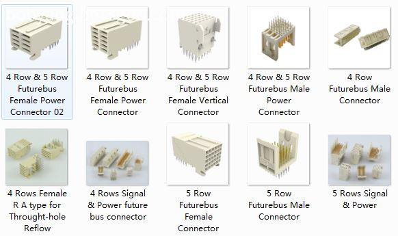
4 and 5 row Future bus Connectors
4 Rows Signal & Power
5 Rows Signal & Power
Female IDC Type 4&5 Rows
Power Connector & Cable
Shroud
Vertical, 5 Rows
Right Aangle, 5 Rows
Vertical, 4 Rows
Right Angle, 4 Rows
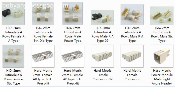
5+2 and 8+2 Hard Metric Connectors

2.0mm Future Bus Connector Male DIP
2.0mm Future Bus Connector Female DIP
2.0mm Future Bus Connector Male Press Fit
2.0mm Future Bus Connector Female Press Fit
2.0mm Future Bus Connector Power Type
2mm HM (hardmetric) Connector Introduction
System designed to meet the current and future needs of instrumentation applications giving excellent electrical and mechanical characteristics. It is a high performance, high density system with flexible configuration which offers upgradeability. The connector system is fully supported by Antenk spice models to guarantee choosing the right product to match the application.
ANTENK 2.0mm HARD METRIC CONNECTOR MODULES comply with international IEC 917and IEC 61076-4-101
standards. The connector systems in telecommunication and other industries require hight density connectors to support
larger amounts of data increasingly higher speeds antenk 2mm hardmetric modules offer the solution
Features and Benefits:
This high density connector modules can be stacked end to end without loss of space.
1,ANTENK developed the 2.0mm series under thorough consideration of impedance match, propagation delay,
cross talk, reflection. It is the ideal connector for digital high speed data application.
2,ANTENK offers differend types with inverted mating configuration. The male connector is a fixed module at the
backplane and the female commector is a free component of the plug-in module. The male connector has 5 signal row.
3 The outer shielding rows z and f of the male connector engage the shielding contacts of the famale connector. theshield
is also designed for gas tight, press-fit installation.
4 The connector system offers 15 contact length that utilize the proven press-fit assembly technique. Within the 15
contact length are 3 mating levels, achievable on both the plug-in and rear I / 0 side.
5 Coding system prevents mix-up and wrong mating between male and female connectors.
6 The 2.0mm hard metric connectors and DIN 41612 connectors can be used on the same PC board as both have the
same mating distance.
7 Staggered make-break pin populations for optional hot-swap capability.
8 Rear pin option for through-the-backplane I/O application.
9 High density PCI capability,shield for EMI/RFI protection.
2mm HM (hardmetric) Connector Features:
High density system with small real estate on backplane and daughtercard
Extensive range of signal, power, coaxial and fibre board-to-board and cable-to-board connections
Modular units give flexible configuration
Special versions for VME64 extensions and CompactPCI
Signal contact rating 1.5a fully energized
Universal power module rated at 7.8A/line, 23.4A fully energized
All lines impedance controlled to 50 (single ended) and 100Ω (differential) nominal
Safe design, complies with IEC950 in mated condition
Universal power module is safe in unmated condition
Several performance levels for board and cable connectors with unshielded and shielded versions
Mismatching keys block mating before any contact touch
Small press fit board hole allows maximum track width and minimum signal corruption
1.4 to 5.6mm (0.055 to 0.220 inch) Backplane thickness range
2mm HM (hardmetric) Connector Applications
Communications & Networking, Computers & Computer Peripherals, Sensing & Instrumentation
Metric Connectors,2.0Mm Hard Metric Connectors,Hard Metric Connectors,Hard Metric Female Connector,2.0mm Future Bus Connector Male DIP,2.0mm Future Bus Connector Female DIP
ShenZhen Antenk Electronics Co,Ltd , https://www.antenkelec.com