Use universal welding board to build MCU minimum system
In this article, we explain another method of using MCU to build a circuit. Use a universal soldering plate to build a single-chip system circuit. Before starting, explain some basic concepts.
Circuit board
First we understand the board. The front panel describes the construction of the circuit board, but in the actual electronic equipment, we usually use the circuit board. The board is mainly used for fixing components and making reliable connections between components.
The circuit board substrate is usually made of non-flammable glass fiber, phenolic resin, bakelite and the like. The circuit connection is made using a copper skin attached to its surface, which is equivalent to a wire; the pins of the component are connected to the copper skin by the molten and solidified metal. The metal used here is usually solder. This process of connecting components and boards is called soldering. The part of the copper plate on the board that is connected to the component pins is called a pad, which is leaking outside before soldering; and those copper pads that are not pads are usually advanced on industrially produced boards. Apply insulating varnish to avoid oxidation, and also facilitate welding (because the molten solder is easy to stick to the copper when soldering, it will not stick to the insulating paint, so the solder will only be on the pad) ).
Single-layer boards have copper on one side and double-sided on both sides. Simple circuits can be used with single or double layers. For some complex circuits, more layers of boards may be used, and there are copper layers inside the board. For example, motherboards for computers and mobile phones usually have many layers.
Previously introduced in-line and patch component packages. In-line packaged devices require a hole in the board. The board has a copper pad on one side and the component pins are plugged in from the other side and soldered to the pad. The chip device does not need to be punched, the pad is on one side of the board, and the component is placed on this side, and the pad is directly aligned with the solder.
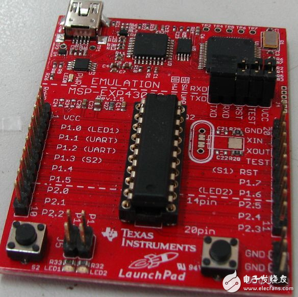
In the figure, the top few pins are densely mounted, and the other are in-line components. The red part in the picture is covered with varnish, and there are several left sides of the XIN and XOUT characters on the right. Soldered pads.
PCB
The boards are divided into two types, one is a printed circuit board (PCB = Printed circuit board) dedicated to one circuit, and the other is a universal universal soldering board.
Mass-produced electronic products are usually implemented using PCBs. The PCB is first designed by computer software, and then mass-produced through a certain process. The copper skin on the circuit board is processed into a characteristic shape (just like the pattern printed on the printer), and it is laid out in a well-designed place. hole. Then, the PCB is directly assembled and assembled on the components, and the welding assembly can also be automatically completed by the pipeline, which greatly improves the production efficiency.
PCB design
Good PCB
Universal Meter,Multi-Function Multimeter,Electronic Multimeter,Electronic Volt-Ohm-Ma Meter
YINTE TOOLS (NINGBO) CO., LTD , https://www.yinte-tools.com