FPGA lookup table implementation principle analysis
PLD chips with this structure can also be called FPGAs: Spartan such as xilinx, Virtex series, etc.
The Look-Up-Table is abbreviated as LUT, and the LUT is essentially a RAM. Currently, four input LUTs are used in FPGAs, so each LUT can be viewed as a 16x1 RAM with a 4-bit address line. When the user describes a logic circuit through the schematic or HDL language, the PLD/FPGA development software automatically calculates all possible results of the logic circuit and writes the result to the RAM in advance, so that each logical input is equivalent to one signal. Enter an address to look up the table, find out the contents of the address, and then output. Below is an example of a 4 input AND gate:
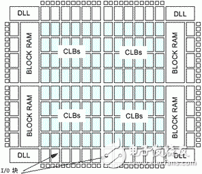
2. Structure of FPGA based on lookup table (LUT)Let's take a look at the internal structure of xilinx Spartan-II, as shown below:

Xilinx Spartan-II chip internal structure

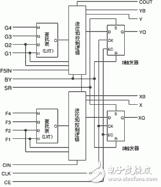
Slices structure
Spartan-II mainly includes CLBs, I/O blocks, RAM blocks and programmable connections (not shown). In spartan-II, a CLB consists of 2 Slices, each slice consists of two LUTs, two triggers and associated logic. Slices can be seen as the most basic structure of SpartanII implementation logic (the other series of xilinx, such as SpartanXL, the structure of Virtex is slightly different, please refer to the data sheet for details)
III. FPGA logic implementation principle of lookup table structure

Let's take this circuit as an example:
A, B, C, and D are input into the programmable connection by the pin of the FPGA chip, and then connected to the LUT as an address line. All possible logical results have been written in the LUT beforehand, and the corresponding data is found through the address. Then output, so the combinatorial logic is implemented. The D flip-flop in this circuit is directly realized by the D flip-flop behind the LUT. The clock signal CLK is input from the I/O pin and enters the clock dedicated channel inside the chip, and is directly connected to the clock terminal of the flip-flop. The output of the flip-flop is connected to the I/O pin and the result is output to the chip pin. Thus the PLD completes the function of the circuit shown in Figure 3. (The above steps are all done automatically by the software, no human intervention is required)
This circuit is a very simple example that requires only one LUT plus a trigger. For a circuit that cannot be completed by a LUT, multiple units need to be connected by carry logic, so that the FPGA can implement complex logic.
Since LUT is mainly suitable for SRAM process production, most FPGAs are based on SRAM process, and the SRAM process chip will lose information after power failure. It is necessary to add a dedicated configuration chip. When powering up, this is the case. The dedicated configuration chip loads the data into the FPGA, and then the FPGA can work normally. Because the configuration time is short, it will not affect the normal operation of the system. There are also a few FPGAs that use an anti-fuse or Flash process. For this type of FPGA, there is no need to add a dedicated configuration chip.
Europe Switch Socket S81 Series
Gold Plug Sockets,Chrome Double Socket,3 Pin Socket With Switch,Brushed Stainless Steel Sockets
Guangdong Jinli Electrical Appliance Co., Ltd , https://www.sokelectric.com