Design Scheme Analysis of Frequency Hopping Radio Transmission System Based on FPGA+DSP
High-rate frequency hopping and high-bandwidth technology are the key to improve the performance of frequency hopping transmitters. This paper proposes a design scheme of frequency hopping radio transmission system based on FPGA+DSP combined with software radio idea and architecture. The system is compatible with multiple modulation methods. And frequency hopping rate and digital rate. The system uses the up and down frequency converter as the frequency converter between the system baseband signal and the intermediate frequency signal, and also gives the system circuit schematic diagram and program flow chart.
introductionFrequency hopping technology is a spread spectrum technology with high anti-interference and high anti-interception ability [1]. The receiving system is a very important part of the frequency hopping communication system. The adaptive frequency hopping technology, high-speed frequency hopping technology, channel coding technology and high-efficiency modulation and demodulation technology have become the new development of frequency hopping technology in recent years. FPGA-based frequency hopping communication The receiving system [2] research has high application value.
Frequency hopping radios use frequency hopping to spread the spectrum and improve anti-interference ability, which has been widely used in military communications [3]. The design scheme of the frequency hopping radio transmission system based on FPGA+DSP [4] has good portability. The modulation and demodulation of wireless communication is complicated, and the digital rate and bit error rate requirements are also different. The transmission system also needs to be able to adaptively detect the clock information and synchronization code of the frequency hopping station, and perform corresponding processing to meet the service rate. Receive demodulation.
The system uses Xilinx's VIRTEX5 XC5VSX50T668 FPGA, which features an advanced high-performance logic architecture that includes multiple hard IP system-level modules and also supports Ethernet and PCI Exprees endpoint modules. The RockeTIO GTP transceiver is designed to operate at speeds from 100 Mb/s to 3.75 Gb/s, and the RockeTIO GTX transceivers are designed to operate from 150 Mb/s to 6.5 Gb/s.
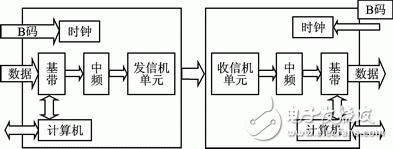
1 system overall architectureThe system works in a half-duplex form, and receives/transmits switching through PTT. The high speed frequency hopping communication system can be embodied as a transmission state model and a reception state model. The hardware device of this system is divided into two entities, one is responsible for sending data, one is responsible for receiving data, and the main software works on baseband board and IF board. The overall framework of the system is shown in Figure 1.

Figure 1 System overall framework
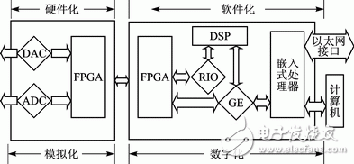
The baseband board chip mainly includes FPGA and DSP. The processor uses the RapidIO interface to exchange data. The intermediate frequency board is mainly composed of FPGA and AD/DA conversion chip. The baseband board and the intermediate frequency board transmit signal data through high-speed SERDES, and the baseband signal is channel-coded and interleaved. Soft spread spectrum, then add the sync header to form a specific frame format, and then write to the FPGA's send message storage area. The structure diagram is shown in Figure 2.

Figure 2 Baseband board and IF board block diagram
As can be seen from Figure 2, at the transmitting end, the data terminal or voice terminal sends the digital information to the baseband signal processor (high-speed general-purpose FPGA + DSP), and then the DSP performs baseband processing on the digital information to obtain a digital baseband signal and send it. Into the FPGA for digital intermediate frequency processing (band shifting process), digitally move the signal to the intermediate frequency, the digitized intermediate frequency signal is converted into an analog signal by a wideband D/A converter, and finally the electromagnetic wave carrying the information via the radio frequency circuit Send in free space.

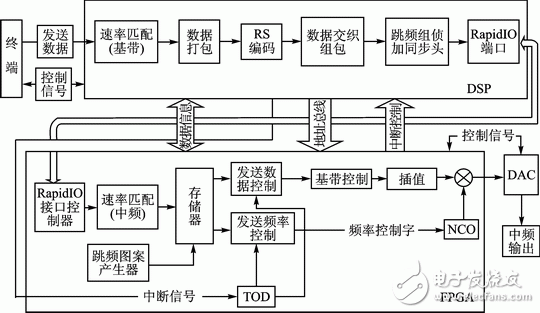
Figure 3 Block diagram of the frequency hopping transmitter

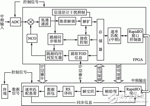
Figure 4 Block diagram of the frequency hopping receiver
After the receiving signal arrives at the receiving end, the analog IF signal passing through the front-end circuit will be converted into a digital signal by the broadband A/D converter, and sent to the FPGA for intermediate frequency processing (the process of moving under the spectrum), after the FPGA is demodulated The digital baseband signal is sent to the DSP. After the receiving baseband processing is completed, the DSP will send the information sequence to the remote voice terminal or data terminal, thus completing a complete communication process.
For the processor, the subject selected TI's DSP chip TMS320C6487TCI and Xilinx's FPGA VIRTEX5 XC5VSX50T668 as the hardware architecture carrier realized by the high-speed frequency hopping system. Xilinx's Virtex5 series uses the second-generation ASMBL (Advanced Silicon Combination Module) column architecture, which includes five distinct platforms (sub-series), which are larger than any previous FPGA series. High, flexible, low power consumption, etc., can quickly complete special operations in digital signal processing.
2 system designThe frequency hopping transmitter system includes a baseband processing part and an intermediate frequency processing part, and the baseband processing part is completed by an FPGA and a DSP. The main processing includes: generating a transmission message, performing channel coding [5], interleaving, packing in a frame format, and writing into the FPGA. The message memory generates parameters such as a frequency hopping pattern, a frequency hopping number, and a time hopping, and writes to the FPGA internal frequency table memory, the frequency hopping number register, and the time hopping register. The IF processing part is completed by FPGA and AD/DA. The main processing includes: memory control, baseband modulation, pulse shaping, digital up-conversion, transmission data control and frequency hopping control. In order to increase the data transmission rate, the processor uses the RapidIO port of the DSP chip for data exchange, and the baseband board and the intermediate frequency board convert data by high-speed SERDES.
Sewing Machine Motor,Dc Motor Sewing Machine,Industrial Sewing Machine,Brushless Servo Motor
LISHUI SHUANGZHENG MOTOR CO.,LTD. , https://www.szservomotor.com