Design scheme of PWM control based on H-bridge cascade inverter
Design scheme of PWM control based on H-bridge cascade inverter
Abstract: This article mainly discusses the implementation method of H-bridge cascade inverter of high-power high-voltage inverter, mainly from the control strategy implemented by PWM in the system, and aims at the implementation methods and performance of several control strategies. Analysis and comparison.
Keywords: H-bridge, PWM;
1 Introduction
H-bridge cascaded multi-level converter adopts the method of multiple power units connected in series to achieve high-voltage output, and its output mostly adopts multi-level phase-shifting PWM control method to achieve lower output voltage harmonics and smaller dv / dt and common mode voltage and smaller torque ripple. In order to achieve high pressure, it is only necessary to simply increase the number of units, and the technical difficulty of this implementation is small. Each power unit is a separate DC power supply, which is independent of each other, and the control of one unit will not affect other units. The main difference between the H-bridge cascade inverter and the single-bridge inverter is the PWM control method. This article discusses the PWM control method of the H-bridge cascade inverter.
2 H-bridge cascade inverter structure
Each power unit is an independent DC power supply, and its design is shown in Figure 1 below:
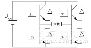
Figure 1 Block diagram of the power unit
According to the description of the power unit in the above figure, the power unit in this implementation mode can generate three levels, namely + Udc, 0, and -Udc. When S1 and S4 are on and S2 and S3 are off, the load gets the voltage + Udc; when S2 and S3 are on and S1 and S4 are off, the load gets the voltage -Udc; when S1 and S3 (or S2 and S4) are on When S2 and S4 (or S1 and S3) are off, the load gets a voltage of 0 (Note: During the control process, it is strictly necessary to avoid the simultaneous conduction of two power devices of the same bridge arm, that is, the two control signal requirements of the same bridge arm are opposite). Therefore, it can be seen that when different PWM control strategies are used, different PWM waveforms can be generated.
3 Carrier phase shift control theory
In general, N-level inverter modulation requires N-1 triangle carriers. In the carrier phase shift modulation method, all triangle waves have the same frequency and amplitude, but the phase of any two adjacent carriers must have a certain phase shift, and its value is
 (1)
(1)
The modulation signal is usually a three-phase sinusoidal signal with adjustable amplitude and frequency. By comparing the modulated wave and the carrier wave, the driving signal of the required switching device can be generated [1].
4 PWM control strategy
The frequency converter usually outputs in the form of a sine wave. For a single-phase bridge, its output can usually be divided into two modes of unipolar modulation and bipolar modulation (limited space, see the reference for specific implementation). The inverter based on the H-bridge method can also output a waveform similar to the output of the single-phase bridge, and its PWM control strategy should be slightly adjusted. The output waveforms of unipolar modulation and bipolar modulation are different in performance. Because unipolar modulation can output three levels, and bipolar modulation can only output two levels, so bipolar The dv / dt of the sexual modulation is larger, which has a greater impact on the motor insulation. In the product design process, the unipolar modulation waveform is usually used as the final output waveform. In this paper, based on the structure of H-bridge cascade inverter and the SPWM generated by the carrier phase shift method as the control signal of each power unit, the unipolar SPWM waveform output is realized. The following discusses and studies several PWM control strategies:
1) Single-arm chopping: the so-called single-arm chopping method is that S1 and S2 are used as half-cycle control signals. When the positive half-cycle is S1, the S2 is turned off; when the negative half-cycle is S1, the S2 is turned on ; The control signal of S3 is SPWM signal,
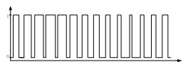
Figure 2 S3 control signal waveform
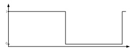
Figure 3 S1 control signal waveform
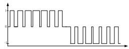
Figure 4 Power unit output waveform
The control signal of S4 is opposite to the control signal of S3. Through such control, the waveform shown in Figure 4 can be output. Although the output waveform is similar to the waveform of the unipolar modulation output of the single-phase bridge and the dv / dt is small, this method results in the power of the two bridge arms balanced.
2) Bipolar modulation: The bipolar modulation of the H-type inverter is the same as the bipolar modulation of the single-phase bridge, the control signal is generated in the same way, the difference is that one is a single bridge arm and the other is a double bridge arm . In order to solve such a problem, the control signals as shown in FIG. 2 are input to S1 and S4, and the signals of S2 and S3 are opposite to those of S1 and S4. In this control method, only a combination of two switching states can occur, namely, S1 and S4 are turned on at the same time, S2 and S3 are turned off at the same time; S1 and S4 are turned off at the same time, S2 and S3 are turned on at the same time. It can output a waveform similar to the single-phase bridge bipolar modulation. Although the dv / dt of the output waveform in this way is large, it will generate higher harmonics and increase the impact on the system, but the power of the two bridge arms of the power unit is balanced, and the control method is simple and easy to implement. In the high-voltage inverter system, there is a distance between the output unit of the control signal and the power unit, and they are connected together by optical fiber. Using this method can reduce the use of optical fiber, reduce the cost of the product, and also reduce The difficulty of field wiring.
3) Unipolar modulation: Although the single-arm chopping method can achieve an output waveform similar to that of the single-phase bridge unipolar modulation, there are inherent defects in this control method, and another control is introduced here the way. As shown in FIG. 1, S1 is controlled by the control signal shown in FIG. 5, S3 is controlled by the control signal shown in FIG. 6, and S2 and S4 are reverse signals of the S1 and S2 control signals, respectively. The control signals shown in FIGS. 5 and 6 are symmetrical SPWM signals with a fundamental phase difference of 180 degrees. Since the phase difference of the fundamental wave is 180 degrees, the duty cycle of the carrier cycle corresponding to the two control signals is 1, which is complementary. There are four combinations of output waveforms: S1 on, S3 off, output + Udc; S1 on, S3 on, output 0; S1 off, S3 off output 0; S1 off, S3 on, output -Udc. As shown in the left part of the dotted line in the figure, the first three kinds of switch combinations will appear, and the latter three kinds of switch combinations will appear on the right side of the dotted line, that is, the PWM wave whose duty ratio meets the sinusoidal change shown in FIG. 7 can be output.
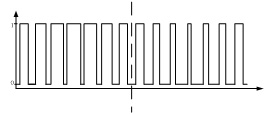
Figure 5 Left bridge arm control signal
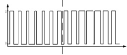
Figure 6 Right bridge arm control signal
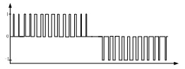
Figure 7 H-bridge unipolar modulation output waveform
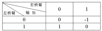
The PWM control realized in this way realizes the conversion from unipolar SPWM to bipolar SPWM, and realizes the power balance of the left and right bridge walls. At the same time, the output voltage harmonics of the inverter obtained in this way are very low. The output does not require a filter and is called a perfect harmonic-free inverter. In inverter control, DSP control is usually used. Since DSP can only output two levels, unipolar SPWM cannot be directly realized, and the assistance of external devices is required. This method uses the combined logical relationship of power units (the logical relationship is shown in the table) 1), replaces the function of the external device, saves the device, reduces the development cost and development difficulty, the control is simple, and it is easy to implement.
Table 1 Logical relationship
5 Conclusion
In the high-power high-voltage inverter technology, PWM control technology is one of its core technologies. A good PWM control strategy is to ensure product performance. In this article, it mainly focuses on the PWM control method of H-bridge cascaded high-power high-voltage inverter. It is discussed, three implementation methods are given, and the implementation methods and performance are analyzed and compared.
Antenk extended its connector product range by SD card connectors. As already mentioned there are various applications, in the past driven by the computer industry, which are using memory cards as well in their end products, single sided pressure contact connectors can be designed and manufactured according to a customer specific requirement based on customer dedicated insulator- and contact dies. Such single sided pressure contact connectors are mainly used as board to board connection on the base of direct contact to the pads on the board.
Compact Flash Card Connector Overview
Store More Memories
Compact Flash storage cards are small, removable, mass-storage devices. They electrically comply with Compact Flash Association standards, the PC Card ATA standard, and run in True IDE mode. These 50-position cards typically hold between 32 MB and 2 GB of memory and are about the size of a matchbook. Antenk`s connectors include headers that can accept Type I (3.3mm thick) or Type II (5.0mm thick) storage cards, flush and raised mounting heights, and ejectors. Antenk Compact Flash card connectors also provide electrostatic discharge protection.Adapter for Compact Flash Card type I and II
Available with various ejectors
Different stand offs heights
Reverse type without stand-off height is not applicable to Compact Flash Card Type II
Compact Flash Card Connector Specification
Insulation Resistance: 1000MΩ at 500V DC
Withstanding Voltage: 500Vrms
Current Rating: 1A AC/DC max.
Contact Resistance: 40mΩ max. at 20mV max.
Operating Temp. Range: -55°C to +85°C
Reflow Solder Temp.: 220°C min. / 60 sec, 260°C peak
Mating Cycles: 10,000 times
Materials and Finish
Insulator: LCP, glass filled (UL94V-0)
Push Button: Glass reinforced PBT (UL94V-0)
SMT Metal: Brass, pure Sn
Pivot Shell: Stainless Steal
Contacts: Brass
Plating: Contacts - Gold (15µ[) over Nickel (40µ[), Solder Tails - pure Sn
Compact Flash Card Connector Product Features
Compact Flash Connectors
Robust surface-mountable designs
Proven PCMCIA contact technology
Accepts hardware for mechanical mounting
Top- and bottom-mounting styles
Right-angle and vertical orientations
Compact Flash Connectors Applications
Desktop and laptop computers
Digital cameras
Smart phones
Data recorders
Slot machines
Industrial and embedded computers
SD Card Connector,Tf Card Connector,Sd Card Connectors,Natural Cf Card Connector,Compact Flash Card Connector,CF cards types I/II,CF Card connector MA type Adapter,CF Card connector MA type Ejector
ShenZhen Antenk Electronics Co,Ltd , https://www.atkconnectors.com