High-speed USB data acquisition system design
In high-speed, high-precision applications such as image processing and transient signal measurement, high-speed data acquisition is required. The USB 2.0 interface has gradually replaced the traditional ISA and PCI data bus with its high speed and other advantages. The hot-swap feature also makes it the preferred interface for various PC peripherals. The EZ-USB FX2 is Cypress's integrated USB 2.0 microprocessor that integrates a USB 2.0 transceiver, SIE (Serial Interface Engine), an enhanced 8051 microcontroller and a programmable peripheral interface. This article will introduce the design of high-speed data acquisition system based on EZ-USB FX2 series CY7C68013 chip. The system has limit protection function, the firmware and driver are easy to write, and can complete high-speed data acquisition and transmission.
Data acquisition system design
The block diagram of the data acquisition system is shown in Figure 1, and the hardware circuit is shown in Figure 2. Among them, AD1674 is a 12-bit analog-to-digital conversion chip, which works in a sequential comparison mode. CPLD is mainly used to control the timing of the ADC and FIFO, control the start and stop of the ADC, and query the state of the ADC. The FIFO acts primarily as a high-speed data buffer.
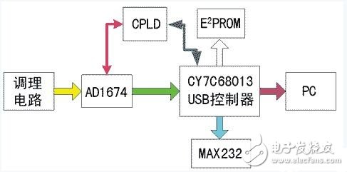
Figure 1 Data acquisition system block diagram
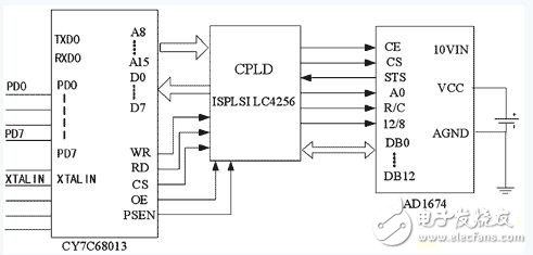
Figure 2 system hardware circuit
CY7C68013 and AD1674 are connected by CPLD to realize the decoding of related control lines and data lines. Under the control of CY7C68013, the AD1674 is first sampled at intervals, and then the result is transferred to the FIFO. When a certain amount of data is collected, the CY7C68013 packs the data to the PC through the USB bus, and the data is processed by the advanced application. The extended RS232 interface can communicate with external devices. At power-on, the CY7C68013 is automatically loaded into the internal RAM from the external E2PROM via the I2C bus for easy firmware modification and upgrade.
The conditioning circuit of the data acquisition front end is shown in Figure 3. This design uses limiting, step-down, filtering, and input impedance enhancement to protect the back-end conversion chip.
Driver and firmware design
The USB device driver is based on WDM. The WDM type driver is a kernel program, which is different from the standard Win32 user mode program and uses a layered processing method. Through it, users do not have to deal directly with the hardware, just access the hardware through the interface provided by the underlying driver. Therefore, the USB device driver does not have to specifically program the hardware, and all USB commands, read and write operations are transferred to the USB device through the bus driver. However, the USB device driver must define the communication interface and communication data format with the external device, and must also define an interface with the application. Cypress provides a complete framework of CY7C68013 driver source code, control panel programs and firmware, which greatly accelerates user development. Users can use existing drivers with little or no modification, and software developers spend a lot of time focusing on application and firmware development. According to the user's own needs, generally only need to modify the DeviceIoControl routine. This design mainly adds control data transfer function, start and stop ADC, reset FIFO and so on. Cypress provides a development framework for CY7C68013, two of which are as follows.
FW.C: FW.C contains the MAIN function of the program framework, which manages the operation of the entire 51 kernel, because the functions of this part have been carefully divided, and generally do not need to be changed.
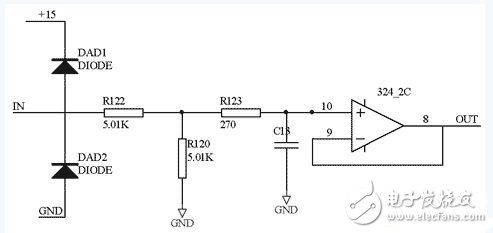
Figure 3 conditioning circuit
PERIPH.C: The user must instantiate PERIPH.C, which is responsible for interconnecting the peripheral devices of the system. The firmware is designed primarily for this file, and the user must instantiate the file to meet the needs of his system to achieve the desired functionality. In the firmware program, the most important ones are the TD_init() and TD_poll() functions. Taking the TD_poll() function as an example, the detection of the external FIFO state and the transmission of data are mainly completed in TD_poll(). The main part of the program is as follows. When debugging firmware, you can use the EZ-USB control panel provided by Cypress.
Void TD_Poll(void)
{
If(GPIFTRIG & 0x80) //Check if GPIF is idle
{
If (EXTFIFONOTEMPTY) / / determine if the external FIFO is not empty
{
If(!(EP24FIFOFLGS & 0x01)) //Check if the FIFO is not full
{
IF(enum_high_speed)
{
SYNCDELAY;
GPIFTCB1=0x02; //Set processing count
SYNCDELAY;
GPIFTCB0=0x00;
SYNCDELAY;
}
Else
{
SYNCDELAY;
GPIFTCB1=0x00;
SYNCDELAY;
GPIFTCB0=0x20;
SYNCDELAY;
}
Setup_FLOWSTATE_Read();
SYNCDELAY;
GPIFTRIG=GPIFTRIGRD|GPIF_EP2;
SYNCDELAY;
While(!(GPIFTRIG & 0x80))
{;}
SYNCDELAY;
}
}
}
}
Pure Sine Wave Inverter,Off-Grid Pure Sine Wave Solar Inverter,Power Inverter For Solar System,Pure Sine Wave Pv Inverter
Zhejiang Kaimin Electric Co., Ltd. , http://www.ckmineinverter.com