SPC563M64L7 main features and block diagram _Discovery Plus development board
ST's SPC563M64L7 is a 32-bit Power Architecture MCU for automotive powertrains. It is a system-on-chip (SoC) with high-performance 90nm CMOS technology with many new features to reduce cost and improve performance. Power Architecture® technology is supported. Additional instructions for DSP, such as enhanced time processing unit, enhanced queued analog-to-digital converter, control area network (CAN) and enhanced module input/output system. In addition, the device also integrates 94KB SRAM and 1.5MB flash memory. The main features of SPC563M64L7, block diagram, and SPC563Mxx series Discovery Plus development board SPC563M-DISP main features and circuit diagram, PCB top layout.
These 32-bit automoTIve microcontrollers are a family of System-on-Chip (SoC) devices that contain many new features coupled with high performance 90 nm CMOS technology to provide substanTIal reducTIon of cost per feature and significant performance improvement. The advanced and cost- The active host processor core of this automoTIve controller family is built on Power Architecture® technology. This family contains enhancements that improve the architecture's fit in embedded applications, includes additional instruction support for Digital Signal Processing (DSP), integrates technologies—such as an enhanced time The processor has a significant level of memory hierarchy consisting of up to 94 KB on-chip SRAM and up to 1.5 MB of internal flash memory. The device also has an External Bus Interface (EBI) for 'calibration'.
Main features of SPC563M64L7:
Single issue, 32-bit Power Architecture® Book E compliant e200z335 CPU core complex
– Includes Variable Length Encoding (VLE) enhancements for code size reduction 
32-channel Direct Memory Access controller (DMA) ï‚·
Interrupt Controller (INTC) capable of handling 364 selectable-priority interrupt sources: 191 peripheral interrupt sources, 8 software interrupts and 165 reserved interrupts.
Frequency-Modulated Phase-Locked Loop (FMPLL) ï‚·
Calibration External Bus Interface (EBI)(a) ï‚·
System Integration Unit (SIU) ï‚·
Up to 1.5 Mbyte on-chip Flash with Flash controller
– Fetch Accelerator for single cycle Flash access @80 MHz
Up to 94 Kbyte on-chip static RAM (including up to 32 Kbyte standby RAM) ï‚·
Boot Assist Module (BAM) ï‚·
32-channel second-generation enhanced Time Processor Unit (eTPU)
– 32 standard eTPU channels
– Architectural enhancements to improve code efficiency and added flexibility 
16-channels enhanced Modular Input-Output System (eMIOS) ï‚·
Enhanced Queued Analog-to-Digital Converter (eQADC) ï‚·
Decimation filter (part of eQADC) ï‚·
Silicon die temperature sensor ï‚·
2 Deserial Serial Peripheral Interface (DSPI) modules (compatible with Microsecond Bus)
2 enhanced Serial Communication Interface (eSCI) modules compatible with LIN
2 Controller Area Network (FlexCAN) modules that support CAN 2.0B ï‚·
Nexus Port Controller (NPC) per IEEE-ISTO 5001-2003 standard ï‚·
IEEE 1149.1 (JTAG) support ï‚· Nexus interface ï‚·
On-chip voltage regulator controller that provides 1.2 V and 3.3 V internal supplies from a 5 V external source.
Designed for LQFP144, and LQFP176
The SPC563Mxx series microcontrollers are system-on-chip devices that are built on Power Architecture® technology and:
ï‚·Are 100% user-mode compatible with the Power Architecture instruction set ï‚·Contain enhancements that improve the architecture's fit in embedded applications ï‚·
Include additional instruction support for digital signal processing (DSP)ï‚·
Integrate technologies such as an enhanced time processor unit, enhanced queued analog-to-digital converter, Controller Area Network, and an enhanced modular input-output system
Operating Parameters
– Fully static operation, 0 MHz
– 80 MHz (plus 2% frequency modulation - 82 MHz)
– –40 C–150 C junction temperature operating range
– Low power design
Less than 400 mW power dissipation (nominal)
Designed for dynamic power management of core and peripherals
Software controlled clock gating of peripherals
Low power stop mode, with all clocks stopped
– Fabricated in 90 nm process
– 1.2 V internal logic 
High performance e200z335 core processor ï‚·
Advanced microcontroller bus architecture (AMBA) crossbar switch (XBAR) ï‚·
Enhanced direct memory access (eDMA) controller ï‚·
Interrupt controller (INTC)
– 191 peripheral interrupt request sources, plus 165 reserved positions
– Low latency—three clocks from receipt of interrupt request from peripheral to interrupt request to processor 
Frequency Modulating Phase-locked loop (FMPLL) ï‚·
Calibration bus interface (EBI) (available only in the calibration package) System integration unit (SIU) centralizes control of pads, GPIO pins and external interrupts.
Error correction status module (ECSM) provides configurable error-correcting codes (ECC) reporting
Up to 1.5 MB on-chip flash memory ï‚·
Up to 94 KB on-chip static RAM ï‚·
Boot assist module (BAM) enables and manages the transition of MCU from reset to user code execution from internal flash memory, external memory on the calibration bus or download and execution of code via FlexCAN or eSCI.
Periodic interrupt timer (PIT)
– 32-bit wide down counter with automatic reload
– 4 channels clocked by system clock
– 1 channel clocked by crystal clock 
System timer module (STM)
– 32-bit up counter with 8-bit prescaler
– Clocked from system clock
– 4 channel timer compare hardware 
Software watchdog timer (SWT) 32-bit timer ï‚·
Enhanced modular I/O system (eMIOS)
– 16 standard timer channels (up to 14 channels connected to pins in LQFP144)
– 24-bit timer resolution 
Second-generation enhanced time processor unit (eTPU2)
– High level assembler/compiler
– Enhancements to make 'C' compiler more efficient
– New 'engine relative' addressing mode 
Enhanced queued A/D converter (eQADC)
– 2 independent on-chip RSD Cyclic ADCs
– Up to 34 input channels available to the two on-chip ADCs
– 4 pairs of differential analog input channels 
2 deserial serial peripheral interface modules (DSPI)
– SPI provides full duplex communication ports with interrupt and DMA request support
– Deserial serial interface (DSI) achieves pin reduction by hardware serialization and deserialization of eTPU, eMIOS channels and GPIO 
2 enhanced serial communication interface (eSCI) modules ï‚·
2 FlexCAN modules ï‚·
Nexus port controller (NPC) per IEEE-ISTO 5001-2003 standard ï‚· IEEE 1149.1 JTAG controller (JTAGC)
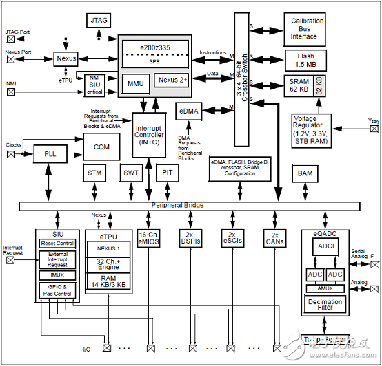
Figure 1. Block diagram of the SPC563Mxx series
SPC563Mxx Series Discovery Plus Development Board SPC563M-DISP
The SPC563M-DISP Discovery kit helps you to discover SPC56 M line Power Architecture® Microcontrollers. The discovery board is based on SPC563M64L7, a 32-bit Power Architecture Book E compliant e200z335 CPU core with 1.5Mbyte on-chip in an LQFP176 package. Singular interfaces including CAN/SCI/K-LINE/DSPI/GPIO make the SPC56M-Discovery an excellent starter kit for customer quick evaluation and project development. The SPC56 M family is designed to address cost sensitive powertrain and transmission applications. The SPC56 M line Key functionality is Time processing units (eTPU) a coprocessor to create events in sync with internal or external signals without flooding the CPU with interrupt to serve.
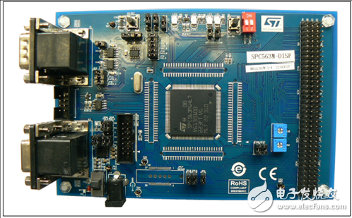
Figure 2. Outline of the Discovery Plus development board SPC563M-DISP
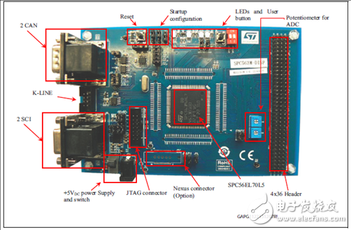
Figure 3. Overview of the Discovery Plus development board SPC563M-DISP hardware
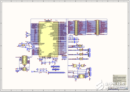
Figure 4. Discovery Plus development board SPC563M-DISP circuit diagram
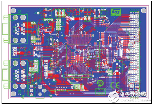
Figure 5. Top of the PCB layout of the Discovery Plus development board SPC563M-DISP
Asic Miner Goldshell:Goldshell KD Max,Goldshell KD6,Goldshell KD6-SE,Goldshell KD Lite,Goldshell KD5 Pro,Goldshell KD5,Goldshell KD-BOX Pro,Goldshell KD-BOX,Goldshell KD2
Goldshell Miner is an industry-leading technology company. The company was founded in 2017, we are focusing on high-performance miners and application fields. In the past few years, Goldshell Miner has successfully completed the R&D, mass production, and sales of multiple miners in LTC, CKB, HNS, Sia and other cryptocurrencies. The headquartered is based in Shanghai, Goldshell Miner has offices in Hangzhou, Hong Kong, Singapore,etc. The current R&D personnel account for more than 70% of the company. The core team has more than 10 years of experience in the integrated circuit field. Aiming to become an excellent blockchain computing power provider, and promoting the development of the industry, Goldshell has established an efficient operation system from algorithm research, batch production and delivery, which based on a strong core team and excellent system capabilities. Goldshell continuously improved the computing performance and competitiveness of products, to provide high-performance and high-reliable computing infrastructure and services for the development of digital economy. Especially our household miner-BOX series, allow more customers to join in the market since our product are small, quiet, affordable, and friendly to beginners so that everyone could start mining at home.
Asic Miner Goldshell,Kd Max 40.2Th,Goldshell kda miner,goldshell kd max,goldshell kd6 miner
Shenzhen YLHM Technology Co., Ltd. , https://www.ylhm-tech.com