Application of GaN transistor technology in power conversion
GaN sailing
HEMT (High Electron Mobility Transistor) Gallium Nitride (GaN) transistors were first introduced in 2004, when Eudyna of Japan introduced a depletion RF transistor. By using gallium nitride on silicon carbide substrates, Eudyna has successfully produced transistors for the RF market. The structure of high electron mobility transistors is described as two-dimensional electron gas (2DEG) based on an abnormally high electron mobility near the interface of ALGAN and GaN heterostructures. Applying this phenomenon to gallium nitride grown on silicon carbide, Eudyna successfully produced a reference power gain in the frequency range of several gigahertz. In 2005, Nitronex introduced the first depletion RF high-transmission transistor, which was first fabricated on a silicon-based GaN wafer using Nitronex's SIGANTICTM technology.
With the participation of several other companies in the market, GaN RF transistors continue to advance in RF applications. However, the acceptability outside this market is very limited, the main reason is the cost of the device and the operation of the depletion device is not convenient.
In June 2009, EPC introduced the first enhanced silicon-based gallium nitride (eGaN?) field effect transistor (FET). This transistor is specifically designed to replace power MOSFET devices. These products can be produced at low cost and in large quantities using standard silicon manufacturing techniques and equipment.
Our most basic requirements for power semiconductors are performance, reliability, control and cost. The structure of any new device cannot be commercialized without these features.
Let's compare silicon, silicon carbide, and GaN devices as next-generation power device development platforms.
Why use GaN devices?
Since the 1950s, silicon has been the main material for power semiconductors. Compared to other early semiconductor materials such as tantalum or selenium, it has four major characteristics:
1. Silicon devices are driving the emergence of new applications;
2. Silicon devices have proven to be more reliable;
3. Silicon devices are easy to use in many ways;
4. Silicon devices are more cost effective.
If a new generation of power transistors is to replace silicon devices, its material properties must be demonstrated to be superior to silicon devices in the above four aspects.
The advantages of silicon devices are based on their fundamental physical characteristics and large investments in manufacturing infrastructure and engineering. Let us now understand some of the basic properties of silicon and how it compares to other alternative materials. Table 1 shows the three main electrical properties of three competing semiconductor materials used in the power management market.
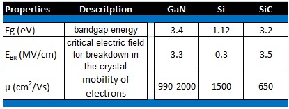
Table 1: Comparison of properties of gallium nitride, silicon carbide and silicon materials
How to compare the performance of power transistors using the above basic crystallization parameters, one of which is to compare the theoretically achievable maximum performance of the above three devices. The many features of power devices have a considerable impact on current power conversion systems. Five of the most important features include device conduction efficiency, breakdown voltage, switching speed, size, and cost. These device characteristics determine the achievable system frequency and power density.
From the data in Table 1 (adjusted for the high mobility of GaN two-dimensional electron gas) we can derive the theoretical minimum resistance (reciprocal of conductance) as a function of breakdown voltage and material.
Table 1 shows that because of the high critical electric field strength of both silicon carbide and GaN devices, their resistance and breakdown voltage have a superior relationship, allowing the device to achieve a smaller size at a given breakdown voltage, and The terminals can be arranged more closely together. In addition, another additional advantage of GaN devices compared to SiC devices is that GaN devices can be smaller at a given resistance and breakdown voltage due to the higher electron mobility of the two-dimensional electron gas. The size of the GaN device adds points!
Since gallium nitride devices can be much smaller than silicon devices and their electron mobility is higher than silicon or silicon carbide devices, gallium nitride high electron mobility transistors can have the advantage of faster switching. Figure 2 shows the transition time of a 12 V to 1.2 V buck converter with a GaN transistor and two silicon power MOSFET devices. The switching time of a GaN transistor is one-fifth that of an equivalent 40 V silicon device and one-fourth that of an equivalent 25 V silicon device. This again adds points to the GaN device!
Transformer For Shore Power Supply
Transformer For Shore Power,Safe Power Supply For Ships,Shore Power Isolation Transformer,Shore Power Transformer
SANON DOTRANSÂ Co., Ltd. , https://www.sntctransformer.com