FET name, parameters, types and pin maps
 The following is a circuit diagram of [Field Effect Tube Naming, Parameters, Types, and Pin Diagrams]
 First, the model name naming method of the field effect transistor The second naming method is CS××#, CS stands for FET, XX represents the serial number of the model, and # represents the different specifications in the same model. For example, CS14A, CS45G, etc.
Second, the parameters of the FET
1. I DSS — saturated drain current. Refers to the drain-source current when the gate voltage U GS = 0 in a junction or depletion insulated gate field effect transistor.
2. UP — pinch-off voltage. It refers to the gate voltage in the junction or depletion type insulated gate field effect transistor when the drain source is just turned off.
3. UT — Turns on the voltage. Refers to the gate voltage in the enhanced insulated gate field effect transistor when the drain and source are just turned on.
4, gM - transconductance. It is a ratio of the gate-source voltage U GS — control capability to the drain current ID, that is, the ratio of the amount of change in the drain current ID to the amount of change in the gate-source voltage UGS. gM is an important parameter to measure the amplification of FET.
5. BUDS — drain-source breakdown voltage. It refers to the maximum drain-source voltage that the FET can withstand when the gate-source voltage UGS is constant. This is a limiting parameter and the operating voltage applied to the FET must be less than the BUDS.
6. PDSM - Maximum power dissipation. It is also a limit parameter, which refers to the maximum drain-source dissipated power allowed when the FET performance does not deteriorate. When used, the actual power consumption of the FET should be less than the PDSM and leave a certain margin.
7. IDSM - Maximum drain current. It is a limit parameter, which refers to the maximum current allowed between the drain and source when the FET is in normal operation. The operating current of the FET should not exceed IDSM
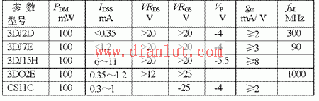
Main parameters of several commonly used field effect transistors
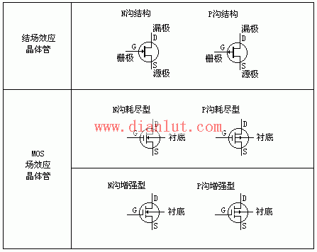
Third, the classification of FETs According to the different channel semiconductor materials, the junction type and the insulated gate type are divided into two types: channel and P channel. If divided by conduction, the FET can be divided into depletion mode and enhancement mode. The junction field effect transistors are depleted, and the insulated gate field effect transistors are both depleted and enhanced.
Field effect transistors can be divided into junction field effect transistors and MOS field effect transistors. The MOS field effect transistor is further divided into N-channel depletion type and enhancement type; P-channel depletion type and enhanced type. See below.
Fourth, the role of FET
2. The high input impedance of the FET is very suitable for impedance transformation. Commonly used in the input stage of multi-stage amplifiers for impedance transformation.
3. The field effect transistor can be used as a variable resistor.
4. The FET can be conveniently used as a constant current source.
5. The FET can be used as an electronic switch.
Fifth, the field effect tube test
1. Pin identification of junction field effect transistor:
The gate of the FET corresponds to the base of the transistor, and the source and drain correspond to the emitter and collector of the transistor, respectively. Place the multimeter in the R×1k file and measure the positive and negative resistance between each two pins with two test leads. When the positive and negative resistances between two pins are equal, both KΩ, the two pins are the drain D and the source S (interchangeable), and the remaining one is the gate G. . For a junction FET with 4 pins, the other pole is the shield (in-use ground).
2. Determine that the grid uses a black meter pen to touch one of the electrodes of the tube, and the red meter pen touches the other two electrodes. If the resistance values ​​measured twice are small, it means that they are forward resistance. The tube belongs to the N-channel FET, and the black meter is also the gate.
The manufacturing process determines that the source and drain of the FET are symmetrical and can be used interchangeably without affecting the normal operation of the circuit, so there is no need to distinguish between them. The resistance between the source and the drain is about several thousand ohms.
Note that this method cannot be used to determine the gate of an insulated gate FET. Because the input resistance of the tube is extremely high, the inter-electrode capacitance between the gate and source is small, and as long as a small amount of charge is measured, a high voltage can be formed on the inter-electrode capacitance, and the tube is easily damaged.
3. Estimate the amplification capability of the FET. Turn the multimeter to R×100, the red meter to the source S, and the black meter to the drain D, which is equivalent to adding 1.5V to the FET. At this time, the hands indicate the resistance value of the DS interpole. Then, the gate G is pinched with a finger, and the induced voltage of the human body is applied as an input signal to the gate. Due to the amplification of the tube, both the UDS and the ID will change, which is equivalent to a change in the resistance between the electrodes of the DS. It can be observed that the hands have a large amplitude of oscillation. If the hand swings slightly when the hand is pinched, the tube's amplification ability is weak; if the hand does not move, the tube is damaged.
Since the 50 Hz AC voltage induced by the human body is high, and the operating points of different FETs measured with the resistance file may be different, the hands may swing to the right or may swing to the left when the gate is pinched by hand. A small number of tubes RDS are reduced, causing the hands to swing to the right, the RDS of most tubes increases, and the hands swing to the left. Regardless of the direction in which the hands are swung, as long as there is a significant swing, the tube has an amplification capability.
This method is also applicable to measuring MOS tubes. In order to protect the MOS field effect transistor, the screw driver insulation handle must be held by hand, and the metal rod is used to touch the grid to prevent the body's induced charge from being directly applied to the grid to damage the tube.
After each measurement of the MOS tube, the GS junction capacitor will be charged with a small amount of charge, the voltage UGS is established, and then the meter needle may not move. At this time, the GS pole is short-circuited.
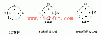
The pin sequence of the commonly used junction field effect transistor and MOS type insulated gate field effect transistor is as shown in the following figure.
 (Editor: Circuit Diagram)
 Electronic Zinc Alloy Die Casting
Electronic Zinc Alloy Die Casting,Custom Die Cast Aluminum,Zinc Alloy Die Casting Stainless,Precision Aluminum Alloy Water Pump
Dongguan Metalwork Technology Co., LTD. , https://www.diecast-pro.com