Detailed explanation of the miniaturized and improved design of the existing anti-metal tag antenna with microstrip structure
0 Preface
Radio Frequency Identification (RFID) [1] is a non-contact close-range automatic identification technology. Its basic principle is to use the energy transmission characteristics of radio frequency signals or electromagnetic field coupling to realize automatic identification of objects. RFID technology has the characteristics of strong anti-interference ability, large amount of stored information, non-contact, long service life, multi-tag identification, and fast response speed. RFID systems have been widely used in public transportation, personnel identification, vehicle management, automatic toll collection, access control management and other fields.
Passive RFID systems are usually divided into low frequency (LF), high frequency (HF) and ultra high frequency (UHF) systems, which are composed of three basic elements: reader, tag and antenna. When designing an RFID system, the RFID system must be considered the background environment. Literature [2]-[4] analyzed the read and write performance of passive UHF electronic tag antennas in complex environments. The read and write performance of tags in different environments will be affected, especially when the tag is attached to the metal surface. hardly ever read. Reference [5] analyzes the reasons for the influence of metal on the tag antenna, and uses a raised tag to overcome the influence of metal, and uses metal to reflect electromagnetic waves to enhance the reading performance of the tag, but the antenna size is large and the antenna performance is not ideal. . Reference [6] adopts the rectangular microstrip patch corner cutting and capacitive coupling feeding technology to realize the circular polarization and broadband characteristics of the microstrip antenna.
In this paper, through the research on the port-enclosed small microstrip antenna [7], the radiation patch is loaded with a short circuit, and high-performance microwave dielectric ceramic [8] is used as the dielectric substrate. Under the premise of sacrificing less gain, it can be Reduce the size of the existing anti-metal antenna [9], and obtain good matching performance. The tag chip is a UHF-RFID tag chip of the EM4235 model, which has an impedance of 18-j178 Ω at a center frequency of 920 MHz.
1 Anti-metal tag structure and implementation
The field between the traditional rectangular microstrip antenna patch and the ground plate has the following characteristics: (1) the electric field has only the Ex component, and the magnetic field has only the Hx and Hy components, that is, the microstrip antenna radiates the TM wave along the z-axis direction; (2) The internal field does not change with the z-coordinate; (3) the current around the edge cannot be directional, that is, the tangential magnetic field at the edge is zero, so the surrounding of the cavity can be regarded as a magnetic wall. Reference [7] seals one port of the antenna cavity with copper foil, as shown in Figure 1, the upper surface of the medium is covered with a radiation patch, the length of the radiation patch is L and the width is W. The left port of the xoz plane is closed with copper foil, thus forming a closed-port microstrip antenna structure.
Since there is no tangential component of the electric field on the ideal metal surface, the plane where the closed port is located becomes an ideal electric wall. Using the cavity theory to analyze the internal field of the antenna, the rectangular microstrip antenna usually works in the TM01 mode (or the TM10 mode), and the resonant frequency of the TMmn mode can be obtained as:
In this paper, a microwave dielectric ceramic with a dielectric constant of 22 and a thickness of 4 mm is used as the dielectric substrate. Microwave dielectric ceramics, which are the key basic materials in current communication technology, are mainly used in UHF and SHF (ultra-high frequency) frequency bands. They have the following advantages: high relative permittivity, which facilitates miniaturization of devices; The small tanδ ensures excellent frequency selection characteristics.
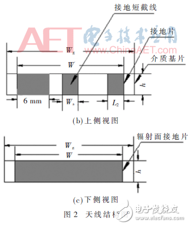
The designed anti-metal antenna is composed of a grounded antenna radiating surface at one end, a grounded stub, two short-circuit clips and a grounding plane. The dielectric substrate is made of microwave dielectric ceramics, with a thickness of 4 mm, a relative permittivity of 22, and an antenna width W of 20 mm. The length L of the radiation patch calculated from equation (3) is about 32 mm, and the distribution of parameters of the antenna is shown in Figure 2. shown. where L is the overall length of the radiation patch, W is the overall width of the radiation patch, Wg is the overall width of the antenna, Li is the length of the plug-in feed microstrip line, Wi is the width of the plug-in feed microstrip line, and Ls is The length of the grounding stub, Ws is the width of the grounding stub, and L2 is the length of the shorting piece at one end.
2 Antenna model theory and equivalent circuit diagram
Before designing each parameter of the antenna, it is necessary to understand the guiding principles of parameter design and the influence of parameter changes on the antenna performance. The antenna model proposed in this paper can be represented by the equivalent circuit model of the transmission line shown in Figure 3.
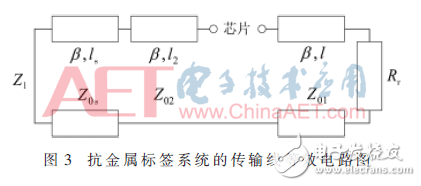
The radiating surface of the antenna, the ground stub and the two ground plates are respectively equivalent to a section of microstrip transmission line, and the feed end is located between the transmission lines.
It can be seen from the above formula that the resistance value of the stub is approximately zero, and the reactance value changes with the length of the stub. When 0 < Ls < 0.25λ, the reactance value is inductive.
According to the above analysis, the equivalent input impedance of the anti-metal antenna is the series connection of the radiating surface impedance, the ground stub impedance and the ground plate impedance. The change of Ls will cause the change of the reactance value of the transmission line. When 0 < Ls < 0.25λ, with the increase of Ls, the reactance value of the transmission line increases from zero to infinity, so the imaginary part of the antenna input impedance can be adjusted by adjusting the size of Ls, but it has little effect on the real part; The adjustment of the real part of the antenna input impedance can be achieved by adjusting L2. In summary, adjusting L2 and Ls can realize the regulation of the real part and imaginary part of the input impedance of the antenna, and it is convenient to complete the conjugate matching between the antenna and the chip.
3 Antenna simulation and result analysis
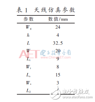
This paper uses the high frequency electromagnetic field simulation soft HFSS13.0 as the simulation tool. Using equations (1) to (9), and through parameter optimization, the optimal design parameters of the antenna can be obtained, as shown in Table 1.
The simulation parameters are defined as follows: Ls and L2 are variable variables, the center frequency is 920 MHz, the sweep frequency range is 820 MHz to 1 GHz, and the step size is 5 MHz. The simulation of the metal environment is replaced by a metal plate of 200 mm × 200 mm, and the port impedance of the antenna is set to be the conjugate of the chip impedance, that is, Z=18+j178 Ω. By adjusting Ls and L2, the optimal conjugate matching between the input impedance of the antenna and the chip is achieved.
The result after using HFSS simulation optimization is shown in Figure 4. At 920 MHz, the minimum value of S11 is -31 dB. At this time, the input impedance of the antenna is 8+j178 Ω, indicating that the impedance matching with the antenna port is excellent. In the frequency band of 860 MHz to 960 MHz, the relative bandwidth of S11 <-15 dB is 11%, indicating that the antenna meets the frequency requirements of different countries. According to the pattern of the antenna, the reading distance of the antenna is calculated by formula (10) [10]:
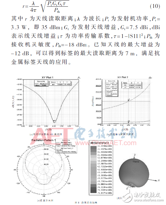
4 Conclusion
In this paper, a miniaturized and improved design of the anti-metal tag antenna with the existing microstrip structure is carried out. Using the structure principle of the port-enclosed microstrip antenna, a new microwave dielectric ceramic is used as the dielectric substrate, and a 32.5 mm×24 The small size of mm×4 mm anti-metal tag antenna meets the requirements of customers for small size, low cost, and anti-metal tag. At the same time, in the 860~960 MHz frequency band, the return loss is S11 <-15 dBm (relative bandwidth 11%) , to meet the broadband requirements. The gain placed on the metal plate is about -8 dBi, which meets the requirements for reading tags at distances greater than 1 m.
Curing Screen Protector,Hydrogel Phone Cutting Machine,Protective Film Cutter Machine,Screen Protcter Custting Machine
Shenzhen TUOLI Electronic Technology Co., Ltd. , https://www.hydrogelprotectors.com