Design and Implementation of GPU Debugging System Based on Dynamic Continuous Data
With the development of GPU technology, the GPU structure has become more and more complex, and the debugging of hardware becomes an increasingly difficult task. The difficulty of hardware debugging lies in the opacity of the hardware itself. When a problem occurs, engineers can't see what's happening inside the hardware like software debugging, nor can they set a breakpoint halfway and stop the hardware like software debugging.
To facilitate debugging of hardware, GPU designers have developed a variety of hardware debugging methods to reduce the difficulty of hardware debugging, traditionally DebugBus, scan path method, ARM CoreSightTM technology. The purpose of these methods is to use some method to expose the internal information of the hardware to the engineer and reduce the opacity of the hardware. However, the exposed information is static information at a certain point in time inside the hardware. The help to the hardware engineer is limited. .
This paper proposes a new debugging architecture. Compared with traditional technologies, it can provide dynamic data to engineers over a period of time, allowing engineers to understand how the internal conditions of the hardware change during this period, enabling engineers to quickly locate Abnormal changes in the problem. Even further, engineers can import the information into the simulation environment and reproduce the hardware problems in the simulation environment.
1 Traditional hardware debugging methods and their defects 1.1 DebugBusDebugBus technology is the first debugging technology introduced in chip design [1-2]. The basic principle is to add a batch of status registers in the hardware design. Each module sends its own status code to this status register. When a problem occurs, the engineer reads the status code in the status register so that the cause of the problem can be analyzed.
The disadvantage of the DebugBus technology is that the bits of the status register are limited, so that the state of the module can be reflected. Engineers can only know the actual status of the module through the status code.
1.2 Testability Design Technique Based on Scan Path MethodThe testability design technique based on the scan path method is an important method of the DFT technology [3-5]. This method can set the state of each flip-flop in the circuit from the outside of the chip, and through the simple The scan chain design scans to see if the trigger is operating in a normal state to detect the correctness of the circuit.
The drawback of this technique is that it is too slow because it is a serial operation and cannot read all data at once, causing engineers to get an instant data [6].
1.3 ARM CoreSightTM TechnologyCoreSightTM technology is a new debugging architecture introduced by ARM in 2004 to provide more powerful debugging capabilities [7].
CoreSightTM technology is more suitable for software debugging because it provides engineers with instructions and register passing sequences between modules. Software engineers can know how the commands they send to the hardware are transferred between the hardware modules. However, hardware development engineers want to know more about complete session information between modules and modules, and even signals within the module [8-9].
2 New debugging system hardware sectionFor hardware development engineers, to debug hardware problems requires a lot of session information between modules and modules in the hardware. This information is preferably continuous information in a certain period of time, rather than a simple point-in-time information.
But to collect all this information for the debugger, you need to solve two problems:
First, the amount of information that is generated every clock cycle is large. In order not to affect the subsequent timing, it must be processed within one clock cycle. However, the limitations of hardware bandwidth determine that these cannot be processed in one cycle. This is also the main reason that in the past technology could only provide brief information.
Second, since a large amount of information is generated every clock cycle, the overall amount of information that we have to deal with is very large, and the storage of this information is a problem.
To solve these problems, a dual clock system was designed. When we discovered that we needed to store information, we stopped the global clock and caused each module to stop working. At the same time we use another set of clock system to drive the debug module to collect and compress information. After the information is collected, relevant data is sent to the storage module for storage. When the storage is complete, reactivate the global clock and let each module continue to work.
Due to the dual clock system, sufficient time is provided for information collection and storage. Therefore, on the storage medium, we gave up the expensive but low-capacity flash memory, instead we chose to allocate a large interval from the on-board memory, so that we could provide storage space with enough information within the cost range. .
Based on the above design, we divided the new debugging system into five modules.
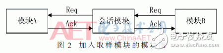
2.1 Session Sampling ModuleThe session sampling module is responsible for passing the session between the module and the module to the session monitoring module or the session recording module. Assume that we have two modules A and B. Under normal circumstances, module A and module B are connected through interface C and pass information to each other, as shown in Figure 1.

The session sampling module is placed on the interface C, and it is used to check whether there is a session between the module A and the module B. If there is a session, the session content is passed to the session storage module, and the content is stored and stored by the session storage module. To the storage medium, as shown in Figure 2.
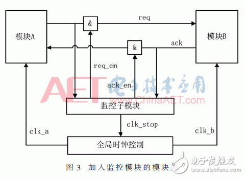
The session monitoring module is responsible for monitoring the sessions between the modules. Once it finds that a session has occurred between module A and module B, the session monitoring module will notify the global clock control module to stop the clocks of all modules, as shown in FIG. 3 .
The session recording module is responsible for recording the contents of the session into memory when the global clock is stopped. We did not use the traditional internal Cache mode, because although the in-memory records are relatively slow, they can provide a large amount of record space and can record a very long session. As long as the memory is large enough, you can record long enough sessions.
The session recording module writes the session record to the memory allocated to the hardware for the software. At the same time, it provides two registers to the software to determine whether there is any information to be written. A register represents the head of unprocessed information in memory, and a register represents the tail of unprocessed information in memory. Before writing the information, the session recording module checks whether the tail of the unprocessed information coincides with the head of the unprocessed information. If yes, the information in the memory is already full, and the recording module will stop waiting for the software to read the information.
Due to the different session sizes between modules, we have not adopted a fixed-length data structure in the stored data structure. Instead, we have designed a variable-length data structure. It is divided into two head and data. The head is a fixed structure, the surface of the packet information, followed by a variable length data stream. It contains three parts of information:
(1) Module ID: Record which module the message came from.
(2) Data length: The size of the session information.
(3) Timestamp: The time when the session occurred can be used for the simulation model.
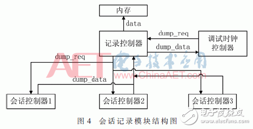
In practical applications, the memory controller has only one input. In order to coordinate the writing order of each module, we specifically designed a recording controller to receive the output of each session recording module and transfer it to the memory controller, as shown in the figure. 4 shows.
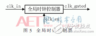
This module is used to control the clock of each module. Once a session record request occurs, the global clock controller sends a clock stop signal to each module, suspends the operation of each module, and sends a clock continue signal after the session recording is completed.
Figure 5 shows the block diagram of the global clock controller. This is the most basic part of the overall architecture design.
When the global clock is suspended, although other modules stop working, a series of modules such as the session recording module, the session sampling module, and the memory controller must continue to work because the system has set up such a clock module for them. When the global clock is aborted, it continues to provide clock interrupts for other modules.
3 The software part of the new debugging systemThe function of the software part is to configure the corresponding debugging environment according to the requirements of the engineer, and store the information generated by the hardware into the corresponding file.
Although the new debugging system solves the problem of long storage time, but in order to improve the debugging efficiency, in the storage process, we use multiple Buffer rotation to improve the data reading efficiency.
4 Results of the applicationA new hardware debugging architecture has been added to the structure of the new generation of GPUs and initial results have been achieved.
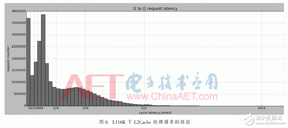
In this design and development, L2Cache was studied using a large number of applications on the FPGA using a new debugging system, and a large amount of data was acquired. Figure 6 shows the results of the post-session analysis between the L2 Cache and the memory storage module (MXU) under different L1Cache designs. From the figure, we can clearly see how L2 Cache handles the received requests and how each of the four banks has their own load. This allows hardware developers to clearly identify problems in the Cache design. And provide a sufficient data base for optimizing the Cache structure.
In addition, we also reproduced some hardware random problems on the FPGA and obtained the corresponding data. After the data was imported into our RTL simulation environment, these hardware problems were successfully reproduced in the simulation environment. Now through the debug system to obtain information for simulation to reproduce, to solve the past hardware developers debugging hardware problems due to hardware package can only be debugged through indirect information analysis. Hardware developers can analyze the cause of the problem based on the waveform and greatly increase the speed of debugging.
5 ConclusionWith this dual clock architecture, we can further develop a single-step debugging system, so that hardware debugging, like software debugging, can set a breakpoint, and immediately check the hardware status after stopping. If it can be achieved, it will further simplify the hardware debugging capabilities and improve the level of hardware development, which is one of our next research directions.
Dc Fan Pcb,Bldc Ceiling Fan Pcb,Bldc Fan Pcb Price,Worcester Bosch Greenstar Fan Pcb
Full Industrial CO.,ltd. , https://www.iotaindustrial.com