Design of Spaceborne Micro GNSS Receiver Using System-on-Chip (SoC) Technology
Aiming at the miniaturization, low power consumption and low cost requirements of Pina satellites for spaceborne GNSS receivers, the design of spaceborne micro GNSS receivers is proposed by using system-on-chip (SoC) technology. In this design, the capture, tracking and positioning solution of the baseband signal are all completed in the SoC, which has the advantages of high integration and high system flexibility. Comparing the designed prototype with the performance parameters of several satellite-based miniature GNSS receivers abroad, the results show that the prototype of the on-board miniature GNSS receiver weighs about 45 g, the size is 100x60 & TImes; 10 mm, and the power consumption is about 3 W. The ability to process GPS L1/L2 and BDS B1/B2 signals can be flexibly configured in multiple modes such as dual-mode single-frequency, single-mode dual-frequency, and dual-mode dual-frequency. The overall performance is better than the existing few on-board miniatures. GNSS receiver.
In recent years, Pina satellites have become a hot spot in international space technology research due to their flexible launch, low cost, high functional density and short development cycle. Due to the limited space of the Pina satellite platform, Global Navigation Satellite System (GNSS) receivers are often the only means of measurement and control for Pina satellites. However, limited by the limited space, limited power and limited cost of the Pina satellite platform, compared with the traditional spaceborne GNSS receiver, the on-board GNSS receiver of the Pina satellite proposes miniaturization, low power consumption and low cost. Wait for higher requirements.
Commercial off-the-shelf (COTS) devices have the advantages of high integration, high density, low power consumption, low price, easy procurement, flexible design, and good performance. In addition, the development of SoC technology enables the integration of functions implemented by multiple discrete devices into a single chip, which has the advantages of low power consumption, high integration, and high system flexibility. Therefore, the application of advanced commercial SoC technology to on-board GNSS receivers can well meet the application requirements of Pina satellites for on-board GNSS receivers.
In the current design of foreign Pina satellite GNSS receivers, both SGR-05U receiver and Plaoenix GPS receiver use GP4020 baseband processing chip, which only contains 12 GPS L1 C/A code correlator channels, and the processing capacity is insufficient. FOTON double The frequency GPS receiver can only process L1 C/A and L2C signals, and uses TI C6457 digital signal processor, which consumes about 4.5 W. The current GNSS receivers based on COTS devices have been widely used in foreign Pina satellites. Most of them use mature GP4020 baseband processing chips or processors and FPGA architectures. However, in China, COTS devices are used to design spaceborne miniatures. The GNSS receiver is still in its infancy. Therefore, it is necessary to develop a spaceborne micro GNSS receiver that uses commercial SoC technology compatible with BDS/GPS signals to improve receiver integration and flexibility and reduce receiver power consumption and cost to meet Pina satellite-to-micro Requirements for GNSS receiver space applications.
This paper introduces the design of the on-board micro-GNSS receiver system using SoC, including the receiver system architecture and the hardware and software co-design method using SoC, and compares the designed prototype with the performance parameters of several foreign satellite-based miniature GNSS receivers. The superiority of the spaceborne micro GNSS receiver designed by SoC technology is verified.
1 Spaceborne Micro GNSS Receiver System Design
1.1 System Architecture
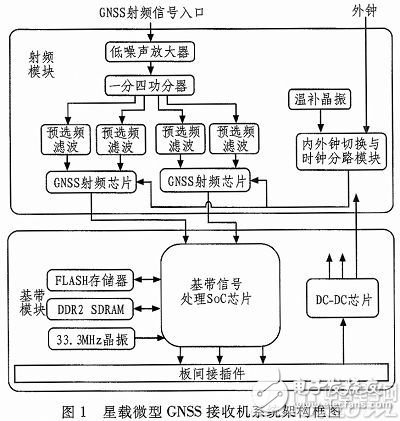
The spaceborne micro GNSS receiver adopts the full COTS device scheme, and the receiver is a single board structure, which is mainly composed of a radio frequency module and a baseband signal processing module, as shown in FIG. The RF module performs amplification, filtering, down-conversion and AD sampling processing of the GNSS signal, and provides the obtained digital intermediate frequency signal to the baseband signal processing module. The RF module clock circuit mainly provides a reference clock for the GNSS RF chip, and can complete internal and external clock switching. The baseband signal processing module performs a series of processing such as acquisition, tracking, bit synchronization, frame synchronization, and positioning solution, and finally sends the positioning result to the number of tube units. The baseband module simultaneously implements DC/DC power conversion to power the RF module and baseband module.
Baseband signal acquisition, tracking and positioning solutions are all completed in SoC, with high integration and high system flexibility. The most critical part of the overall system design is SoC software and hardware co-design.
1.2 SoC software and hardware co-design
The SoC contains ARM hard core processor, programmable logic and a variety of peripheral IO resources. The processor communicates with the programmable logic part and peripheral IO interface through the on-chip AXl4 bus. The system architecture of integrated processor and programmable logic is provided. The IO bandwidth, processing efficiency, and power estimation that traditional dual-chip (external processors and FPGAs) cannot provide. The SoC has the advantages of high performance, flexible configurability and miniaturization of low power consumption. It can be used for spaceborne micro GNSS receivers to meet the needs of Pina satellites.
The software and hardware collaborative design technology adopts the idea of ​​parallel design and collaborative design, and the design efficiency is greatly improved. The development cycle of the satellite-based micro GNSS receiver can be greatly shortened, and the batch production of the receiver can be completed, which meets the requirements of fast response, rapid assembly and fast launch.
1.2.1 SoC hardware design
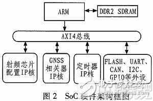
Figure 2 shows the entire SoC hardware architecture. As the core functional unit of the SoC, the ARM processor is responsible for the configuration and communication of peripheral resources such as UART, CAN, I2C, GPIO, and FPGA on the AXI4 bus on the SoC, and undertakes the task of navigation information processing. The RF chip configuration code and the correlator code are encapsulated as IP cores. The ARM processor configures the working mode of the RF chip through the RF chip configuration IP check, so that it works in the GPS L1/L2, BDS B1/B2 working mode. The accumulated data acquisition interrupt signal is generated by the AXI TImer IP core under the control of the ARM processor. The clock of the AXI TImer IP core is provided by the bus clock. The GPS/BDS navigation information processing correlator code is also packaged as an IP core that is attached to the AXI4 bus.
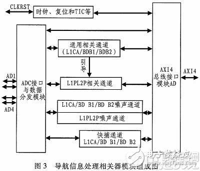
The GPS/BD2 navigation information processing correlator mainly performs carrier stripping, code stripping and correlation accumulation of GPS L1/L2 and BD2 B1/B2 signals, and sends it to the processor to complete the signal acquisition tracking loop processing. The navigation information processing correlator is mainly composed of a fast capture module, a general related channel module, an L1PL2P related channel module and a noise channel module, and the flow between the modules is as shown in FIG. 3 .
In the construction of the SoC hardware environment, the accumulated data acquisition interrupt directly adopts the timer IP core, completes the timing under the control of the processor, periodically generates an interrupt signal, and completes the timely acquisition of the accumulated amount. The RF chip configuration module is also encapsulated into a user IP core. The RF chip is configured in the initialization phase and configured as GPS L1/L2 and BD2 B1/B2 channels. It has been verified that the custom RF chip configuration module can be directly reused, effectively reducing design complexity and improving design efficiency.
After the hardware environment is built, netlist and bitstream files can be generated in EDK XPS (Xilinx Platform Studio).
1.2.2 SoC navigation information processing software design
The navigation information processing software processes the channel accumulation data and the channel measurement data by controlling the digital channel correlator, and completes the acquisition tracking and positioning solution of the GPS and BDS navigation signals, and can provide the user time, position, and time per second. Speed, and output to the manifold system through the interface. The navigation information processing software module is mainly divided into a loop processing module, a positioning solution module, a star selection and parameter prediction module, and a data exchange module. Figure 4 shows the information flow diagram between the navigation information processing software modules of the onboard micro GNSS receiver.
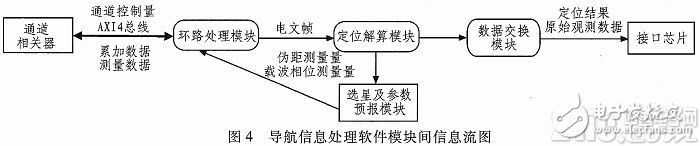
After the loop processing module completes the initial acquisition of the navigation star signal, the signal is accurately tracked and synchronized, and the signal is demodulated into the original telegram frame. The specific operations to be completed include: accurate code tracking, accurate carrier tracking, bit synchronization, and teletext frame synchronization.
The function of the positioning and solving module is to process the information of the carrier phase, the code phase, the number of carriers, the transmission delay, the navigation satellite almanac and its time stamp provided by the loop processing module, and obtain the pseudorange, the pseudorange rate of change, and the navigation. Satellite clocks and navigation satellite almanacs, satellite ephemeris and other measurement information, using these measurement data for navigation and positioning to determine the user's current motion state (including three-dimensional position coordinates, three-dimensional velocity coordinate components, etc.) and time information.
The function of the star selection and parameter prediction module is to provide a search basis for the channel, that is, to predict the navigation satellites that can be captured and the corresponding Doppler shift.
The function of the data exchange module is to output the positioning result and the original observation data to the digital pipe subsystem according to the data communication protocol.
Completion of the navigation information processing software code, after generating the binary executable file in the EDK SDK (Software Development Kit), the software and hardware collaborative design can be performed, and the generated hardware platform file, the board level support package file and the bit in the SDK. The files are collaboratively debugged. After debugging, the .mcs file can be generated and burned into the flash.
2 principle prototype
Figure 5 shows the prototype of the onboard micro GNSS receiver implemented by SoC technology (compared with a smartphone in the market). The receiver size is 100x60x10 mm, the weight is about 45 g, and the power consumption is about 3 W. Compatible with GPS L1/L2 and BDS B1/B2 signals, which meets the application requirements of the Pina satellite to the receiver.
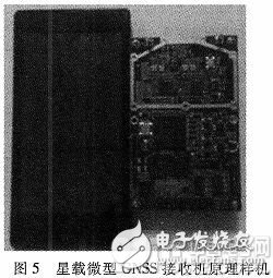
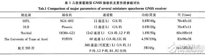
Table 1 shows the main performance comparison between the on-board micro GNSS receiver implemented by SoC technology and several foreign micro GNSS receivers. From the results in the table, the size of the miniature GNSS receiver implemented by SoC technology is comparable to that of the OEM4-G2L receiver, which is slightly larger than the other three receivers; the quality is comparable to that of the SGR-05U receiver and the OEM4-G2L receiver. Phoenix receiver is slightly larger, but much smaller than FOTON receiver; power consumption is smaller than FOTON receiver, larger than the other three receivers; channel number is less than FOTON receiver, but more than the other three receivers, SGR-05U receiving The machine and the Phoenix receiver can only process the L1C/A code, the OEM4-G2L receiver can process the L1C/A code and the L2 P code, the FOTON receiver can process the L1 C/A code and the L2C code, and the on-board micro GNSS implemented by the SoC technology. The receiver can process L1 C/A code, L1 P code, L2 P code, B1 civilian code and B2 civilian code, which has stronger processing capability and more flexibility. It can be seen that the comprehensive performance of the on-board micro GNSS receiver realized by SoC technology is better than the other existing on-board micro GNSS receivers.
3 Conclusion
In this paper, a spaceborne micro GNSS receiver implemented by SoC technology is designed for the application requirements of Pina satellite. The spaceborne miniature GNSS receiver has the characteristics of small mass, small size and low cost, and is compatible with processing GPS L1/L2 and BDS B1/B2 signals, and can complete dual mode single frequency, single mode dual frequency, dual mode dual frequency and the like. The configuration of the mode can provide accurate positioning and timing services for spacecraft such as Pina satellites.
- [Worldwide Compatibility]With a worldwide 100-240V AC input, it's a truly global charger and perfect for international traveling. Compatible with iOS, Android, & Windows smart phones as well as tablets, speakers, cameras, and other 5V USB devices
-
With 9 years experience in the filed, Shenzhen WAWEIS Technology Co., Ltd is one of the best power supply device manufacturer in China. Our world-class production plant passed ISO9001:2008 & ISO14001:2004 certifications and is equipped with the state-of-art technology and machines. The main products we make are power adapters, which can be used in laptop, LCD display, LED lights, CCTV camera(12v series), Speaker(24v series), Balance car(42v series). All our products comply with European environmental standard as well as CCC,RoHS ,CE , FCC.
Ungrouped,High Quality Ungrouped,Ungrouped Details, CN
Shenzhen Waweis Technology Co., Ltd. , https://www.huaweishiadapter.com