PCI-Express bus introduction interface design and implementation
The PCI Express bus is a new generation of I/O local bus standard and is a revolutionary bus architecture that replaces the PCI bus. The PCI bus used to be a milestone in the history of PC architecture development. However, with the continuous development of technology, some new external devices have higher requirements on transmission speed and bandwidth. These factors were not considered at the beginning of PCI design. The requirements of these external devices are not fully met. It is in this context that the PCI Express bus came into being.
A PCI Express connection can be configured with data bandwidths of x1, x2, x4, x8, x12, x16, and x32. Xilinx's Virtex5 family of FPGAs embeds the PCI-Express-Endpoint BLOCk hard core, making it possible to implement a single-chip configurable PCI-Express bus solution.
Based on the PCI-Express interface protocol and the PCI-Express Endpoint Block hard core, this paper uses the Virtex5LXT series XC5VLX50T FPGA chip to design the PCI-Express interface hardware circuit, and now the YPCI-Express x4 bus data transmission.
1 PCI-Express Bus OverviewPCI-Express is a high-performance, general-purpose I/O interconnect technology that can be used in a wide range of computing and communications platforms. Compared to the traditional PCI/PCI-X bus, PCI Express replaces the PCI-X parallel interface with a high-speed serial interface; it replaces PCI-X bus-based communication with point-to-point Switch-based switched communication; Replace the TPCI-X bus-based transport protocol with a packet-based transport protocol (PACketbased protocol). In addition, it introduces new features: enhanced power management, quality of service control (QoS), hot plugging, and sophisticated error handling and recovery.
1.1 PCI-Express Device/Topology
The typical topology of PCI-Express is shown in Figure 1. Three devices are defined in the PCI-Express protocol: RootComplex, Endpoint, and Switeh.
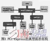
The location of the Root Complex in the system is similar to the host bridge in PCI-X, which is the root of the I/O hierarchy, which connects the CPU and MM to the I/O components. Each Root Complex can have one or more PCI-Express Ports (Root Ports), each defining a hierarchical domain. Endpoint is a PCI-Express endpoint device that can be divided into PCI-Express Endpoint and LegacyEndpoint.
Switch is a PCI-Express switching device. It can be understood as logically composed of multiple PCI-PCI bridges, each of which corresponds to one SwiSh port. From the perspective of configuration software, Swi-tch is a PCI or PCI bridge with two or more logics.
1.2 PCI-Express hierarchy
The three-layer structure is defined in the PCI-Express protocol: TransacTIon Layer, Data Link Layer, and PhysICal Layer. Its structure is shown in Figure 2.
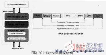
The transaction layer is mainly responsible for grouping and unpacking, and is responsible for managing credit-based flow control.
The data link layer is primarily responsible for link management and data integrity management, including error detection and error correction.
The physical layer contains all the circuitry of the interface: driver and input buffering, parallel-serial-serial-to-parallel conversion, phase-locked loop, impedance matching circuitry, with interface initialization and maintenance. The physical layer can be further subdivided into a logical physical layer and an electrical physical layer (EleCTRical Physical Laycr). The logical physical layer is responsible for receiving packets from the data link layer in the transmission direction, and transmitting the uplink after processing; in the receiving direction, it is responsible for forwarding the packets received from the link to the data link layer. The electrical physical layer is the analog interface to the link and contains the differential transceiver for each channel.
1.3 PCI-Express package
Corresponding to the three-tier structure defined by the protocol, PCI Express defines three packages:
(1) TLP: Corresponds to the transaction layer, mainly completing the memory transactions, I/O transactions, configuration transactions, and message transactions defined in the protocol.
(2) DLLP: Corresponds to the data link layer, mainly used for link management functions, including ACK/NAK protocol, power management and flow control information exchange related to TLP acknowledgement. At this level, a point-to-point link retransmission mechanism and link layer ECC check are provided, providing a reliable fault tolerance mechanism.
(3) PLP: Corresponding to the physical layer, capable of supporting link training of the physical layer, clock tolerance/compensation, and autonomous hardware power management.
Introduction to 2Virtex-5LxtConsidering the cycle, difficulty, cost and other factors of implementing PCI Express bus, this paper uses Xilinx's 65nm process Virtex5 LXT series chip to realize PCI-Express bus interface and application.
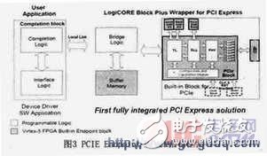
The Virtex 5 Lxt PCIE Endpoint block has full PCI-Express functionality and is fully compliant with PCIe Base Specification v1.1. As a hard core inside the FPGA, it is a configurable PCIe endpoint solution that greatly increases design flexibility and reduces The RNE cost of the design, and support for 1x, 2x, 4x or 8x channel implementation, provides an effective way for system expansion.
The PCIE Endpoint block embedded in the series integrates the physical layer (PHY), data link layer (DLL) and transport layer (TL) in the PCIE protocol, and it also implements the function configuration register of the PCI-Express device. As shown in Figure 3, the following interfaces are included: clock and reset interface, configuration and status interface, power management interface, user interface, and transport layer interface. The PCIE Endpoint block completes the rigorous testing steps of the PCI-SIG Compatibility Symposium, ensuring product compatibility and reducing risk; integrating the Rocket IO-TMGTP transceiver, which provides 100Mb/s to 3 .2Gb/s serial connection performance, can support the 2.5Gb/s rate required by PCI-Express protocol, compatible with PCI-Expre-ss protocol 2.5Gb/s working mode per channel, which makes it in data The codec meets the requirements of the PCI-Express protocol. This article uses the XC5VLX50T chip in this series to design PCI-Express interface hardware circuit to realize PCI-Express x4 data transmission.
The hardware of this paper is mainly to realize the PCI-Express bus interface of the single chip XC5VLX50T, and design the specific application in the FPGA to complete the test and use of the PCI-Express bus interface. The application implemented in this paper has the following characteristics:
(1) The host starts and stops the DMA operation by controlling the internal register file of the FPGA, and supports the full-duplex DMA reading and writing of the endpoint to the root.
(2) PCI-Express bus interface design using Endpoint BLOCk Plus generated by LogICORE. The hard core integrates the physical layer and data link layer resolution in the PCIE protocol, and provides a transport layer interface (TRN) for the designer to process the corresponding transaction layer data packet.
(3) The PCI-Express bus interface supports the implementation of the x4 channel, and the host operating system is the embedded Linux 2.6.10 system. PCI-Express interface testing is also performed under Windows XP.
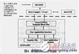
FPGA is the most critical part of the whole design, mainly: PCI-Express hard core; realizes the timing logic of PCI-Express transmission local bus in hard core user interface and transmission interface; and completes DMA control timing logic in its internal. The FPGA is the channel for PCI-Express bus interface and application module data transmission. Use the embedded MPC8548 as the host system application CPU on the Host side, and design the corresponding driver and application program to debug the FPGA internal code. Figure 4 is a topological block diagram of the system.
In the Endpoint Block Plus generated by LogiCORE, two base address memory spaces are defined, one for the DMA register operation and one for the user logic space. This paper mainly introduces the implementation of the user application layer interface, which will process the corresponding transaction layer data packet through TRN.
The user application layer interface mainly includes the following modules: a. TX Engine module; b. RX Engine module; c. Egress Data Presenter module; d. Read Request Wrapper module; e. DMA Control/Status Registers module. The topological relationship between these modules is shown in Figure 5.
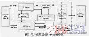
TX Engine: This module is mainly used to generate and send transaction layer data packets: posted transaction package (memory, I/O, configuration read and write transaction), non_Posted transaction package (the bus transaction package is divided into two steps, the first is the sending direction The receiving end submits the bus read and write request, and then the receiving end sends the completion packet to the transmitting end and the compleTIon (complete) packet. The module completes DMA read and write requests by sending posted memory writes, non_Posted memory reads, and receiving compleTIon packets. The startup of this module is controlled by the DMA Control/Status Registers module. The module further includes a plurality of submodules: a posted PACket generator module, a non posted packet generator module, a compleTIon packet generator module, and a transmit TRN state machine module. The three generator modules are controlled by a transmit TRN state machine module, and the control signal of the state machine is controlled by the transmit TRN state machine module. From the Endpoint Block Plus core and the DMA Control/StatusRegisters module.
RX Engine: This module is mainly used to receive the transaction layer data packets sent by the Endpoint BlockPlus module from the RX TRN interface, parse different transaction packets, and perform corresponding processing according to the corresponding packages. The module can handle the following three transaction packages: Complete the package, the memory read package, and the memory write package. The module further includes the following sub-modules: a receiving TRN state machine module, a receiving TRN monitoring module, a receiving data state machine module, and two fifos for storing received data of the completed package and the destination and source addresses of the completed package and the length of the data packet. Used to set the various states in the DMA Control/Status Registers module. The receiving TRN state machine module is only responsible for the status of the data packet at the TRN interface and receiving the receipt, and sends it to the following module; the receiving TRN monitoring module is responsible for allocating data and status according to different TLP packets, and is directly carrying the data completion package. The data is written to the user application interface fifo, or the read request or the write request TLP packet is notified to the TX engine, and the corresponding packet is sent out or notified to the DMA controller for corresponding DMA transfer control; the received data state machine module correspondingly receives the received data. Processing.
Egress Data Presenter: This module is a module for sending data to the TX Engine module. The data to be sent to the host is processed in this module. The data bit width between it and the TX Engine module is defined as 64 bits.
Read Request Wrapper: This module is mainly used for communication control interface between TX Engine module and RX Engine module. In this paper, the possible data length of each DMA read/write operation is: 1KDW, 2KDW, 3KDW, 4KDW, 8 KDW, Optional between 16 KDW. This selection is done by the host by writing a register file for length policy selection.
DMA Control/Status Register: This module is mainly used by the host system to start and stop the DMA read and write operations of the endpoint to the root by controlling the setting of the register file inside the FPGA. It includes a control register and several configuration registers. The configuration register has the host's destination address, source address information, local destination address, source address information, and packet length per DMA. All state machine control is initiated by the state of the bit in the control register, so the control register is the key signal for the entire operation.
3V Lithium CR Series Button Cell
DADNCELL 3V lithium-manganese buckle-type disposable battery adopts manganese dioxide with very stable chemical properties as positive materials and lithium with very high energy as negative electrode materials.
DADNCEL batteries have excellent safety performance, good sealing performance, stable discharge voltage and long storage life. At the same time, they have the characteristics of temperature and wide. The battery can work normally at -20°C ~ +60 °C. Therefore, it is often used in backup memory power supply of some products, such as computer motherboard and automotive alarm. Tire tester, handheld computer, industrial control motherboard, calculator, watch, shoe lamp, electronic thermometer, electronic toys, flashlight, tax control machine, medical device, small electronic gift, Bluetooth wireless products, multifunctional wireless remote control, PDA, MP3, electronic key, card radio, IC card, smart home Electrical, digital camera, mobile phone and other equipment.
All types of batteries developed by DADNCELL Lab do not involve any heavy metals in production, use and waste. They are green and environmentally friendly and can be disposed of with domestic waste.
3V Lithium Cr Series Button Cell,3V Lithium Coin Battery Long Lasting,Button Bettery For Carkeys,Batteries Offer Premium Performance
Shandong Huachuang Times Optoelectronics Technology Co., Ltd. , https://www.dadncell.com