Power Management Chip Pin Description_Power Management Chip Application
Power Management Chips (Power Management Chips) are chips responsible for the transformation, distribution, detection, and other power management of electrical energy in electronic equipment systems. It is mainly responsible for identifying the amplitude of the CPU power supply, generating a corresponding short moment wave, and promoting the power output of the subsequent circuit. Common power management chips include HIP6301, IS6537, RT9237, ADP3168, KA7500, and TL494.
Power Management Chip Basic TypeSome of the major power management chips are dual in-line chips, and some are surface mount packages. The HIP630x series chips are relatively classic power management chips designed by Intersil, a well-known chip design company. It supports two / three / four-phase power supply, supports VRM9.0 specification, voltage output range is 1.1V-1.85V, can adjust the output for 0.025V interval, switching frequency up to 80KHz, with a large power supply, small ripple, internal resistance Small features, can accurately adjust the CPU power supply voltage.
1. The power management chip can also be programmed without current, and the current can reach up to 800mA;
2. In the process of use, no external components, such as diodes, sense resistors, etc., can be used alone;
3, the circuit in the off mode can also support the passage of current, only need to reach 25uA current;
4, when charging can be set to no trickle charge mode, can play a power-saving effect. To make charging faster, use constant-current and constant-voltage charging with over-temperature protection. This charging method does not have to worry about overheating.
5. When starting, soft start can be used to effectively limit the inrush current and prevent the device from being damaged during startup.
1, VCC power management chip power supply
2, VDD gate driver supply voltage input or primary control signal for power supply
3, VID-4CPU and CPU power management chip VID signal connection pin, the main indication of the chip's output signal, so that the two field tube output the correct working voltage.
4, RUNSDSHDNEN start working pin of different chips.
5, PGOODPGcpu core power supply circuit normal work signal output.
6, VTTGOODcpu external nuclear power supply normal signal output.
7, UGATE high-end field control signals.
8, LGATE low end field control signal.
9. The PHASE phase voltage pin is connected to the overvoltage protection terminal.
10, VSEN voltage detection pin.
11. The FB current feedback input is the size of the detected current output.
12. COMP current compensation control pin.
13, DRIVEcpu external nuclear field tube drive signal output.
14, OCSET12v power supply circuit over-current protection input.
15, BOOT secondary drive signal device over-current protection input.
16, VINcpu external nuclear power conversion circuit power source chip connection pins.
17. The output of the VOUTcpu external core power supply circuit is connected to the chip.
18, SS chip delay control terminal, generally connected to the capacitor.
19, AGNDGNDPGND simulated ground power ground
20, FAULT over-consumption indicator output, for its power loss: If the temperature exceeds 135 degrees, high level turns to low level indicating that the chip is too depleted.
21. SET adjusts current limit input.
22, SKIP mute control, grounding for low noise.
23, TON timing selection control input.
24, REF reference voltage output.
25, OVP overvoltage protection control input pin, grounding for normal operation and overvoltage protection, even VCC loss of overvoltage protection.
26, FBS voltage output remote feedback sensor input.
27. The STEER logic controls the second feedback input.
28, TIME / ON5 dual-use capacitance and open or close control input
29, RESET resets the output V1-0v jump, reset when low.
30, SEQ selects the order of PWM power level shifter: 5v output is before 3.3v when SEQ is grounded. SEQ is connected to REF and 3.3v5v are independent. When SEQ is connected to v1, 3.3v is output before 5v.
31, RT timing resistor.
32, CT timing capacitor.
33, ILIM current limit threshold adjustment.
34, SYNC oscillator synchronization and frequency selection, 150Khz operation, sync connected to GND, 300Khz connected to the REF, with 0-5v driven sync frequency to 340-195Khz.35, VIN voltage input
36, VREFEN reference voltage
37, VOUT voltage output
38, VCNTL power supply
Power Management Chip Application AreaThe power management chip has a wide range of applications. The development of a power management chip is of great importance for improving overall performance. The choice of power management chips is directly related to the system requirements, and the development of digital power management chips also needs to overcome cost difficulties. The development of power management chips is of great significance for improving the overall performance. The choice of power management chips is directly related to the demand of the system, and the development of digital power management chips also needs to overcome cost difficulties.
In today's world, people's lives are inseparable from electronic devices for a moment. The power management chip is responsible for the transformation, distribution, detection and other power management of electrical energy in the electronic equipment system. The power management chip is indispensable to the electronic system, and its performance has a direct impact on the performance of the entire machine.
LNK564 power management chip typical application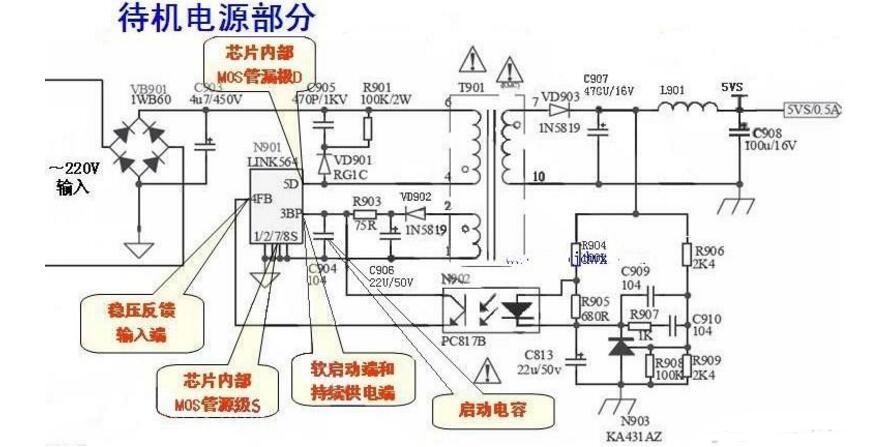
The principle of power supply part: Standby master power management chip adopts LNK564, built-in 700V MOS field tube, switching transformer is T901, LNK564 is a quasi-resonant control chip, and a 5.8V regulator is integrated in LNK564.
Start-up process: AC 100 ~ 240V input voltage is rectified by the rectifier bridge filter, the output voltage of the transformer T901 secondary output terminal by the switch 5.8V, enter the N901 (LNK564) 3 feet (BP), the foot external 100nF bypass The capacitor is used to store the startup voltage. When the BP level reaches the chip startup level, LNK564 starts to operate.
CCD Gel Imaging System Filters
Gel Imaging system can be used in preservation of molecular biology and bioengineering research. Also it can be used in such data Processing as molecular weight calculationsity quantification density scan PCR quantification. we can supply filters for Gel imaging system.
Specification:hard coating
Substrate:BK7 , Fused Silica etc.
Blocking range: 200-1200 nm
Transmittance:>90%
Blocking:<10-4
Ccd Gel Imaging System Filters,Od4 Optical Filters,620Nm Bandpass Filters,590Nm Filters
Zoolied Inc. , https://www.zoolied.com