High current hot swap application with TPS2393A
abstract
The TPS2393A integrated circuit is a hot-swap controller optimized for -48V systems. The TPS2393A is widely used in many applications and has the following powerful features:
Wide input power range
Programmable current limit
. UV / OV protection
. Insertion detection
. Power good indication
. Alarm
The TPS2393A has load current slew rate control that manages the current of the surge load and has peak current limiting. Under normal conditions, the actual rated load current is always less than the safety margin current limit threshold. However, in some cases, the application needs to get a larger rated current into the load. This situation can cause significant stress on the FET used to control the application of inrush current (for example, a system requiring -48V at 10A rated current). At initial turn-on, if the current is limited to 10A (possibly 480W initially), the VDS of the FET is 48V. Of course, as the VDS decreases, the power also decreases. This makes FET selection for this application a very big problem.
This article introduces you to a simple and efficient way to solve this problem, a simple way to extend the scope of the TPS2393A application.
introduction
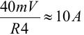
The TPS2393A is a full-featured -48V hot-swap power management IC. Like the most popular hot-swap controllers, the TPS2393A uses an external N-channel power FET and a low-value current-sense resistor to control the load power-up, which acts as a controlled current. Figure 1 is a block diagram of the circuit. The reference voltage is used for the non-inverting input of a linear power amplifier (LCA). The load size information is transmitted to the inverting input as the voltage drop of the sense resistor RSNS. The LCA converts the bypass FET gate to limit the load current to a reference value. The VREF reference is controlled at 40mV as shown in Figure 2. Therefore, during conduction, the current in the load is limited to
The value obtained. (IMAX is the maximum load current.)
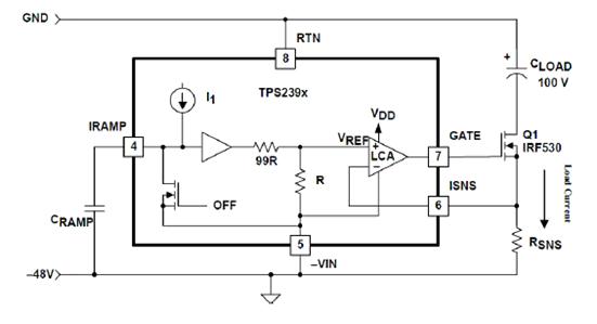
Figure 1 TPS2393 current control loop

Figure 2 ramp generator module
Figure 3 shows a typical hot swap diagram. Figure 4 shows the waveform of 2A current limit.
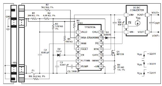
Figure 3 Typical hot swap diagram
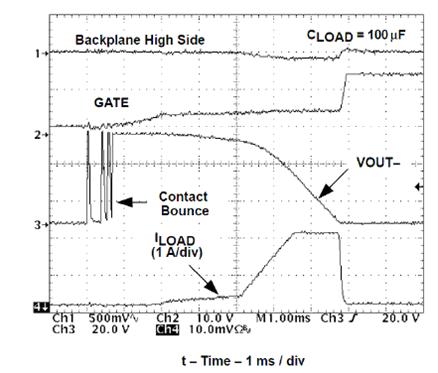
Figure 4 TPS2393 waveform
Please note:
VOUT is actually the VDRAIN of the FET. At T = 0, the VDS is approximately 48V; when the FET is turned on, it is close to zero. Contact flickering shows hot plug or board insertion events. This is why the left side of the VDS is 0 (the board is not powered). After insertion, the voltage swings and then rises to 48V. The gate begins to switch and allows current to enter the board, during which time the VDS decreases as the IDS increases.
Achieve heavy load hot swap
To avoid violating the high load current safe operating area (SOA) curve, the maximum current level must be limited when the inrush current reaches a reasonable value.
For example, during turn-on, the typical charging current for bulk capacitors is 2A (40mV/20mohm); therefore, the actual load current must be less than 2A, as shown in the top of Figure 4. However, in some applications, the load current can be much higher, ranging from 5A to 50A, as shown in the lower panel of Figure 4. Of course, this requires that the value of the sense resistor RSNS is very low to allow the maximum current limit to enter the load. However, at these high currents, IMAX is also very high. It is difficult to choose the correct current limiting FET. For example, the normal load current is 10A and the RSNS value must be less than 4mohm (40mV/10A). IMAX will also exceed 10A.
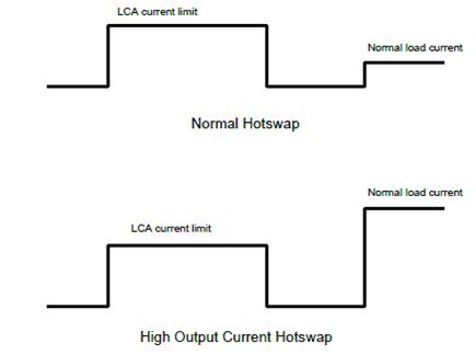
Figure 5 different ideal current waveforms required
Assuming a normal load current of 10A, and considering the thermal rise of the FET, we should choose a correct RDSOn. For example, select FDB047N10: Rdson = 4.7mOhm; Rθja = 62.5 °C / W;
Assuming the ambient temperature is TA=40°C, the junction temperature of the FET is calculated as follows:
In steady state, there is no problem with the increase in heat. In addition, it is necessary to look at the SOA map to determine if the FET can handle transient power dissipation at startup. Figure 5 shows the typical maximum SOA for the FDB047N10.
Under the 25° C-shell temperature and 48V input conditions, the 10A constant current should be shorter than 1mS (see the red dotted line in Figure 5), but it can support 2A constant current running time of about 10mS (see the blue dotted line in Figure 5). . In another approach, a small current requires more time to charge the bulk capacitor to the input voltage. Therefore, we should make a trade-off between reliability and charging time to choose a suitable current level.
Also keep in mind that the SOA map in the FET product data sheet is based on a 25 ° C ambient case temperature; in an actual power system, the ambient case temperature will be higher, so we must consider lowering the rated temperature. The application note "Using the TPS2490/91 Hot-Swap Design and Transient Thermal Response of FETs" is a good reference.
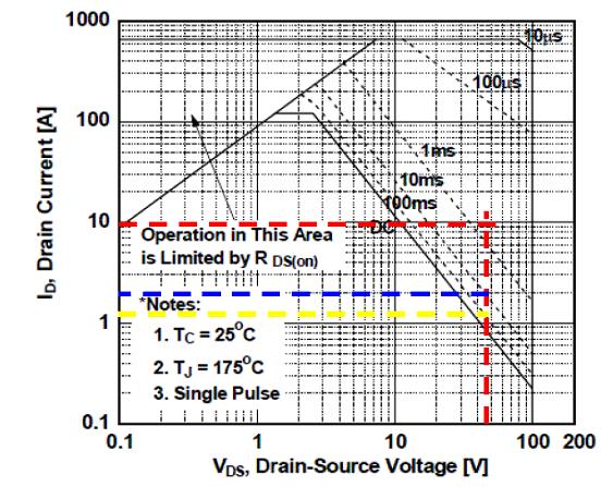
Figure 6FDB047N10 SOA curve
A simple way to meet high output current hot swap requirements is to isolate the LCA current limit threshold from the overcurrent (OC) limit threshold. However, they are integrated in the TPS2393A.
After reading the product manual carefully, we can see that the power good status indicator pin (/PG) is active low when the following conditions are met:
The DRAINSNS pin voltage is below the power good threshold (1.35V).
The IRAMP pin voltage is higher than 5V.
Therefore, in the LCA current limit condition and overcurrent condition, we can use the /PG signal to change the current level of the bypass FET. Figure 6 is a simplified schematic view.

Figure 7 adds bias current to change the actual load
Since we know that the ISENS pin is the negative side of the LCA (controlled at 40mV), we can get the following equation:
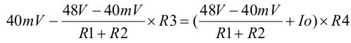
Io can be simplified to:

In Fig. 6, R1 = R2 = 470K, R3 = 680 ohm, and R4 = 4mohm. Therefore, at startup, the actual load current Io ≈ 1.3A. From the SOA curve shown in Figure 5 (see the yellow dotted line), the maximum SOA time for a constant load current of 1.3A is close to 100 mS.
Assuming the total output capacitor CLoad = 100μF, the minimum charging time is:
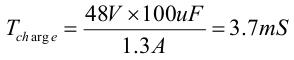
The TPS2393A can also program the "surge slew rate" via a capacitor on the IRAMP pin, so the actual charging time will be longer. The load capacitor charging time is less than the maximum SOA time, so the FET is suitable for current design.
The TPS2393A also includes a programmable "fault timer" to protect the FET. From the previous analysis, we can set the "fault time" in the range of 3.7mS to 100mS. We can calculate the timer capacitor using the following equation:
Figure 7 shows the startup waveform, which has been tested on the EVM board.
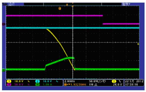
Figure 8 Bias current start
When the startup process is completed, the /PG signal goes low. The bias current flowing through R2 is negligible and the maximum load current will rise to
.
Since R1 is directly connected to the bus voltage, the bias current varies with the bus voltage. If the bus has a wide voltage range, we can add an external circuit to provide a fixed reference voltage to R1 so that the bias current will also be fixed.
in conclusion
Although the TPS2393A has only a relatively low current limit threshold, it can be used for more applications as long as the load current at steady state is higher than the charge current during the start-up ramp. This article describes a way to change the current limit at different stages of operation (from rising to stable).
references
1. TI SLUS536C "TPS2393A Product Manual"
2, "Using the TPS2393 -48V ATCA module hot swap", the author: Jim Bird, TI SLUA318
3. "Full Featured -48V Hot Swap Power Manager (TPS2392 and TPS2393)", Author: Andy Ripanti, TI
4, "Using TPS2490 / 91 hot-swap FET transient heat dissipation design and response" by: Martin Patoka, TI
5, "FDB047N10 Product Manual", Fairchild Semiconductor Corporation
Pv Combiner Box,Photovoltaic Combiner Box,Solar Power Combiner Box,Pv Array Combiner Box
Zhejiang Kaimin Electric Co., Ltd. , https://www.ckmineinverter.com