Detailed explanation of the oscilloscope's DDC (digital down conversion) technology
Nowadays, with the increasing complexity of electronic product design and the increasingly complex test content, people may not only need to know the time domain characteristics of the signal, but also the frequency domain characteristics of the signal, or the joint characteristics of multiple domains. As a result, it is very likely that the working test bench is full of instruments: oscilloscopes, spectrum analyzers, etc., the workspace is crowded, and more importantly, the test work becomes complicated, the complex connections of various instruments, instruments The synchronization problem needs to be solved... Therefore, for general debugging measurements, people hope to have a multi-function instrument that can meet the requirements of time domain testing, frequency domain analysis, and even time-frequency domain signals for joint debugging of coherent, and even It can also be analyzed for some vector signals. Oscilloscopes are widely used as the most basic test and measurement instruments. If they can be integrated into these analysis functions, they will bring great convenience to engineers. At present, each oscilloscope manufacturer has also introduced some all-in-one oscilloscopes, and the technology is also different. It is not a separate time domain and frequency domain channel measurement, and it is analyzed by software calculation, so it also faces some problems. For example, in spectrum analysis, we know that RBW (resolution bandwidth) is inversely related to the capture time of the signal. If a small RBW is required (commonly speaking, the spectrum is more fine), it takes longer to capture time, and the sampling rate is inevitable. Will be reduced, then the signal for high frequencies will not be analyzed. Conversely, if you want to analyze high-frequency signals, the RBW will be larger and the frequency resolution will be weaker. In addition, in vector signal analysis, the storage space and sampling rate of the oscilloscope are also limited, which makes it impossible to analyze signals for a longer period of time. So how do you solve the problems in these measurements with oscilloscope design? This paper introduces the DDC (Digital Downconversion) technology used by R&S oscilloscopes, which solves the above problems well and brings the multi-domain joint test to the fullest.
02
DDC Introduction
DDC (Digital Down Converter) is a digital down conversion. It is a sine or cosine signal generated by the NCO (Numerical Control Oscillator) at the same frequency as the RF or IF signal carrier, multiplied by the RF or IF signal, and finally obtained by baseband filtering and resampling. The process of the signal.
Due to the huge advantages of digital signal processing, it has been widely used. In wireless communication systems, it is also increasingly desirable to convert A/D (analog-to-digital) and D/A (digital-to-analog) signals closer to the RF front-end, thereby enabling various functions in communication through digital signal processing. However, due to the development level of ADC (analog-to-digital converter) and DSP (digital signal processor), it is very difficult to perform AD conversion and digital signal processing directly on the very high frequency RF end. The same is true for digital oscilloscopes. Processing capacity limitation, if the high-frequency signal is AD sampled at the RF end, a high sampling rate is required. Once the capture time is lengthened, the sample points will be very large. At this time, it will be found that the oscilloscope processing time becomes longer and the response is slow. To resolve this conflict ADC and the DSP, using the DDC signal to baseband frequency, and then using a lower rate of resampling, the data amount can be reduced to improve the efficiency of DSP.
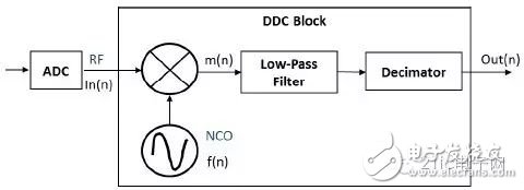 Figure 1 DDC block diagram
Figure 1 shows the DDC block diagram, which consists of NCO, mixer, low-pass filter and resampling modules. The RF signal passes through the high speed ADC and becomes the digital signal In(n):
In(n) = s(n)×cos(wn) (1)
Where s(n) is the signal, cos(wn) is the carrier, and w is the carrier frequency. The NCO generates a local oscillator signal f(n) with the same frequency as the RF signal: f(n) = cos(wn) (2)
The local oscillator signal is multiplied by the RF signal to obtain the signal m(n): m(n) = In(n) × f(n) = s(n) × cos(wn) × cos(wn) = 1/ 2s(n)[cos(2wn)+1] (3)
After the signal m(n) is low-pass filtered and resampled, the output signal Out(n) is obtained: Out(n) = 1/2s(n) (4)
It can be seen that, through DDC, the true useful signal s(n) is retained, and the amount of data is greatly reduced by resampling, thereby improving the efficiency of subsequent signal processing. Similarly, if DDC technology is used in a digital oscilloscope, not only can the useful signal in the RF signal be preserved, but also the amount of data can be greatly reduced, and the processing speed of the oscilloscope can be improved.
Let's discuss the DDC application in an R&S oscilloscope.
03
RDC implemented by R&S oscilloscope hardware
Before discussing DDC applications in R&S oscilloscopes, let's compare the differences between R&S digital oscilloscopes and traditional digital oscilloscopes.
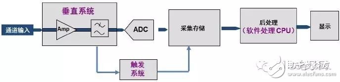
Figure 2 Block diagram of a traditional digital oscilloscope
Figure 2 is a block diagram showing the basic structure of a conventional digital oscilloscope. The signal enters the oscilloscope through the analog channel, and is converted into a digital signal by the ADC through the vertical gain amplifier and filtering. It is stored by the acquisition and storage module, and then processed by the software for subsequent processing, and finally displayed on the oscilloscope screen. Traditional digital oscilloscopes use software processing for data processing, and there is no DDC structure on the hardware. Therefore, when collecting or spectrum analysis of some high-frequency signals, it must be performed at a high sampling rate. Since the storage space of the oscilloscope itself is limited, the time length of the acquired or analyzed signals is relatively short.
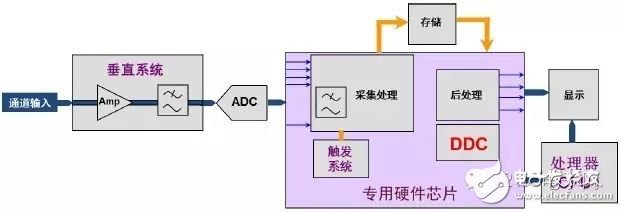
Figure 3 R&S digital oscilloscope block diagram
Figure 3 shows the basic block diagram of the R&S digital oscilloscope. The signal processing flow is not much different from traditional digital oscilloscopes, but uses more hardware structures, including triggering systems, digital processing, and DDC. The features and advantages of other hardware structures are not discussed in this article, but it is obvious that the hardware implemented DDC is used in the structure. Thanks to the hardware DDC structure, the signal can be downconverted to baseband and resampled at a lower sampling rate. In the same storage space, signals can be collected or analyzed for longer periods of time. And because it is a hardware implementation, the speed will be faster.
Below, the application of DDC in I/Q demodulation and spectrum analysis is discussed.
3.1 DDC in I/Q demodulation
Let us first look at a problem encountered in a real test: the signal to be tested is a modulated signal with a carrier frequency of 300 MHz and a modulation bandwidth of 2 MHz. Then, if the signal is collected by an oscilloscope, it is desirable to collect the time as long as possible, and how long can the signal be collected for a long time? For this problem, we analyze from the perspective of signal analysis.
First of all, for such modulated signals, military radar signals (such as chirp signals), civilians have general communication signals (such as QAM signals), most of which are vector signals. For the analysis of such signals, quadrature demodulation, i.e., I/Q demodulation, must be used. Traditional digital oscilloscopes can only directly collect RF signals for this type of signal. After the data is stored, it can be processed by special software or programmed by third-party software (including I/Q demodulation and subsequent processing).

Figure 4: Traditional digital oscilloscope processing signal processing
Figure 4 shows the processing flow of a conventional oscilloscope for this type of modulated signal. For the above problem, the carrier frequency is 300MHz and the modulation bandwidth is 2MHz, then the highest frequency of the signal is 301MHz. According to the Nyquist sampling theorem, the sampling rate used by the ADC must be 2 times or more of the highest frequency of the signal to truly restore the waveform. We assume that the traditional oscilloscope ADC uses 2 times the highest frequency, that is, the sampling rate of 602MSa/s for sampling. The sampling rate of the oscilloscope using exactly 2 times is generally not recommended, and the relationship of 3~5 times is generally used to restore the waveform more realistically. Assuming that the oscilloscope has a memory depth of 10 MSa, the maximum time that the signal can be acquired is 10 MSa / (602 MSa/s) ≈ 16.6 ms.
That is, using a conventional oscilloscope to collect such signals, only signals of more than 10 milliseconds can be acquired. If the signal is higher for the carrier frequency, such as 2GHz, the acquisition time will be shorter.
For the above problems, the R&S oscilloscope uses a hardware-implemented I/Q demodulation module, the most important part of which is DDC. By using this module, it is possible to acquire a modulated signal for as long as possible.
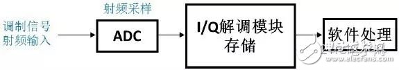
Figure 5 R&S digital oscilloscope processing signal processing
Figure 5 shows the processing flow of the modulated signal by the R&S oscilloscope. The I/Q demodulation module is shown in Figure 6.
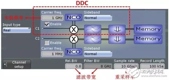
Figure 6 R&S digital oscilloscope I/Q demodulation module
The R&S digital oscilloscope always maintains the RF signal at the highest real-time sampling rate (such as 10GSa/s or 20GSa/s), converts it into a digital signal, and then digitizes the digitized RF signal through the I/Q demodulation module. The digital down-conversion and filtering obtain the baseband signal with lower frequency, and finally reduce the amount of data by re-sampling, store it and send it to the software for processing.
The I/Q demodulation module is mainly composed of DDC, including NCO, multiplier, low-pass filter and resampling, as shown in Fig. 6. The NCO is responsible for generating the local oscillator frequency, which is set at “Carrier freq.â€. Generally set to the same frequency as the RF carrier, after setting, the NCO and the two signals with the same orthogonal frequency are generated. The two orthogonal signals are respectively multiplied by the radio frequency signal, and two orthogonal baseband signals are obtained by filtering. The filter bandwidth can be set at "Rel.BW". Set the resampling rate at "Sample rate" and finally resample the baseband signal. Through this kind of processing, one can eliminate the processing process of performing I/Q demodulation in software. More importantly, when the oscilloscope has limited storage space, it can store signals for longer analysis. For example, for the problem at the beginning of this section, for a carrier frequency of 300MHz and a modulation bandwidth of 2MHz, by setting "Carrier freq.", the local oscillator frequency is the same as the carrier frequency, which is 300MHz. After the down-conversion, the signal becomes baseband, and the bandwidth is Only 2MHz. The resampling rate "Sample rate" setting is also calculated in a 2-fold relationship, so just set to 2 × 2 = 4 MSa / s. The memory depth is still assumed to be 10MSa, so the signal time that can be acquired and analyzed is 10MSa / (4MSa/s) = 2.5s !!! The length of time is increased by more than 150 times!
For such efficient use of storage space, some of my friends are very surprised, and it is somewhat difficult to understand. It may be considered that even with the addition of the DDC structure, digital signal processing is still present, and there is still an ADC at the front end. That is to say, the oscilloscope still needs to sample the RF signal at the front end, and still needs to satisfy the Nyquist theorem twice as much as the RF signal. Then, only 16.6ms of the signal can be stored, and where is 2.5s. We will carefully analyze the signal processing flow to know the reason.
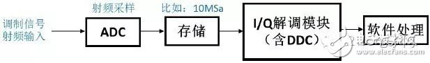
Figure 7 Generally considered signal processing flow
The general signal processing flow is shown in Figure 7. For this structure, as understood above, even if DDC is used in this case, the signal collected by the RF needs to be stored first, so it is still affected by the high sampling rate. For the above example, only 16.6ms of signal can be stored. But the real processing flow of the R&S oscilloscope is shown in Figure 8.
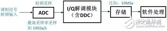
Figure 8 R&S oscilloscope signal processing flow
At the RF front end, the ADC maintains the highest real-time sampling rate, such as 10GSa/s, so that it does not cause signal aliasing. The sampled digital signal is sent directly to the DDC for digital down conversion. Since the DDC of the R&S oscilloscope is implemented in hardware and is fast, it can be processed in real time and stored directly after processing. Through this real-time DDC processing, the storage space can be saved very well, and the 2.5s signal storage as described in the above example can be realized.
In this regard, we conducted the following experiment.
First, a radio frequency pulse signal with a carrier frequency of 3 GHz is generated by a signal source, the modulation pulse width is 0.4 ms, and the pulse repetition period is 1 ms. The settings are shown in Figure 9:
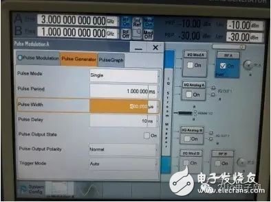
Figure 9 Pulse modulation RF signal setting with carrier frequency of 3GHz
For the acquisition and analysis of this signal, if a conventional digital oscilloscope is used, the result of the signal length that can be acquired and analyzed is equivalent to that shown in Figure 10:
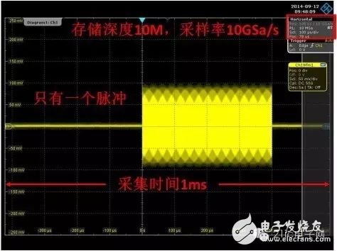
Figure 10: Traditional digital oscilloscope to collect RF pulse equivalent results
Since the RF signal frequency is 3 GHz, the sampling rate is at least 6 GSa/s or more, and we set it to 10 GSa/s. The storage depth is still set to 10M. It can be seen that only the signal of 1ms can be collected at this time, that is, a pulse signal can be collected and analyzed as much as possible.
If using an R&S oscilloscope with an I/Q option with a DDC structure for acquisition analysis, we can first set the local oscillator frequency to 3 GHz, and after the signal is converted to baseband, it can be acquired at a lower sampling rate, such as setting to 100 MSa. /s, the storage depth is also set to 10M. The setting is shown in Figure 11:
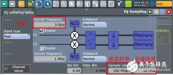
Figure 11 R&S oscilloscope I/Q option settings
At this point of observation, we can collect and analyze signals for a longer period of time, that is, 100ms, that is, we can collect and analyze up to 100 pulse signals! If the resampling rate is set lower, we will be able to acquire and analyze the signal for a longer time. Figure 12 shows the R&S oscilloscope test results:
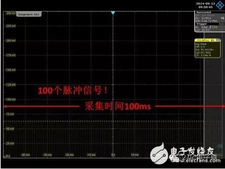
Figure 12 R&S oscilloscope to acquire RF pulse results
In summary, the DDC technology in the R&S oscilloscope I/Q option enables efficient use of limited memory space for acquisition and analysis of signals of maximum length in RF signal acquisition and analysis.
3.2 DDC in spectrum analysis
The spectrum analysis function of the oscilloscope generally adopts FFT (Fast Fourier Transformation) or fast Fourier transform. The block diagram of the spectrum analysis of a traditional digital oscilloscope is shown in Figure 13.
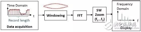
Figure 13 Traditional digital oscilloscope spectrum analysis block diagram
After the analog signal passes through the ADC, it becomes a digital signal. Then, different window functions are selected for windowing. Finally, the FFT is directly used to transform the signal into the frequency domain. The spectrum obtained by this processing method ranges from 0 Hz to the maximum frequency (usually equal to half the sampling rate of the ADC). For example, the ADC sampling rate is 5 GSa/s, and the FFT obtains a spectrum ranging from 0 Hz to 2.5 GHz. If you want to observe the spectrum of a certain segment, the spectrum is amplified and displayed to the frequency band by means of a software display zoom. The advantage of this traditional oscilloscope spectrum analysis method is that all processing is calculated by software, and the algorithm is simple, so it is easy to implement. But if you are looking for faster real-time spectrum measurements or more accurate spectrum analysis, this traditional approach can be very difficult. Due to the full software processing and always calculating the entire frequency range (0 Hz to maximum frequency), the processing speed will be slow and real-time or near real-time spectrum analysis will not be possible. In addition, the oscilloscope setting will be very complicated, and it is necessary to constantly adjust the time domain parameters (such as time base, sampling rate, etc.) to meet the required frequency domain parameter settings. Most importantly, it is limited by the oscilloscope's memory depth, and the number of FFT points usually used is only a few K. Therefore, the frequency resolution, that is, the minimum distinguishable frequency will be very limited, and it is usually difficult to achieve an ideal frequency resolution.
In general, frequency resolution has two explanations. One explanation is that the minimum frequency spacing between two adjacent frequency points in the FFT is shown in equation (5): ∆f = fs / N = 1 / t (5)
Where ∆f represents the frequency resolution, fs represents the ADC sampling frequency, N represents the calculated number of points of the FFT, and t represents the length of time of the acquired signal, that is, the acquisition time. It can be seen that the longer the signal acquisition time t, the smaller the frequency resolution ∆f, that is, the better the frequency resolution.
The second explanation is that the frequency resolution can be expressed in terms of resolution bandwidth (RBW). RBW is defined as the main function 3dB bandwidth of the window function, as shown in Figure 14:
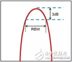
Figure 14 RBW definition
If the difference between the two signal frequencies is less than the defined bandwidth, RBW, then the two frequencies will be mixed and cannot be resolved.
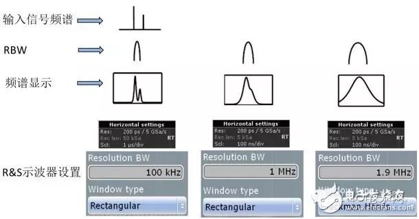
Figure 15 Different spectrums corresponding to different RBW settings
Figure 15 shows a completely different spectrum obtained by setting different RBWs for the input signal of the same spectrum. From left to right, the RBW increases sequentially. It can be seen that the width of the main lobe is also increased in turn, and the frequency resolving power is also sequentially decreased. When it is to the far right, the two frequencies in the signal are completely indistinguishable.
Since the effects of DDC on the two interpretations of frequency resolution are similar, we will only discuss the case of the second interpretation, RBW. The RBW calculation method is as shown in the formula (6): RBW = RBWnorm × fs / N = RBWnorm / t (6)
Among them, RBWnorm is the normalization factor of the window function, such as the Blackman-Harris window is 1.8962, fs is the sampling frequency, N is the FFT calculation point, and t is the signal acquisition time length. It can be seen from equation (6) that for a fixed window function, in order to increase the frequency resolution, that is, to reduce the RBW, it is necessary to increase the acquisition time of the signal, that is, the acquisition time. As can be seen from Fig. 15, for a fixed rectangular window, the RBW is reduced from 1 MHz to 100 kHz, and the time base setting is increased from 100 ns/div to 1 μs/div. But for digital oscilloscopes, the memory depth is limited. And the following relationship exists between the storage depth and the capture time and the sampling rate: storage depth = sampling rate × capture time (7)
As can be seen from equation (7), for a fixed memory depth, the sampling rate and the capture time are inversely related. If you want to increase the capture time, it means that the sampling rate will drop. If the sampling rate is reduced, it will mean the risk of aliasing. That is to say, for the spectrum analysis of the traditional digital oscilloscope, if the frequency resolution is to be improved, the risk of signal aliasing will be faced, or only the analysis of the low frequency signal can be performed; if the analysis of the high frequency signal is to be performed, the sampling rate is guaranteed. Then the frequency resolution cannot be improved.
For this contradictory relationship, the R&S oscilloscope introduced a series of processing methods such as DDC to solve the problem well.
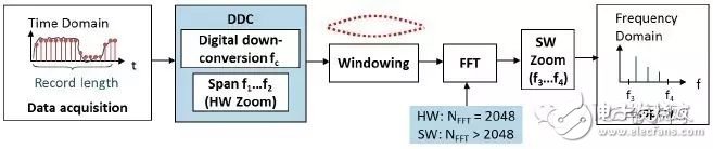
Figure 16 R&S digital oscilloscope spectrum analysis block diagram
Figure 16 shows the spectrum analysis flow for the R&S oscilloscope and Figure 17 shows the spectrum analysis setup block diagram.
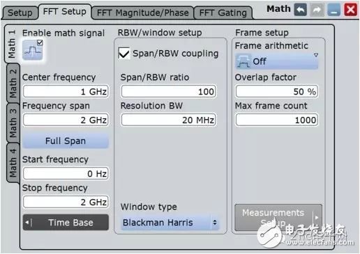
Figure 17 R&S Digital Oscilloscope Spectrum Analysis Settings
Compared to traditional digital oscilloscopes, R&S oscilloscopes introduce DDC modules that downconvert the signal to baseband before FFT. Setting the center frequency Center frequency is equivalent to setting the local oscillator frequency to down-convert the signal to the baseband. Therefore, when the baseband signal is resampled, the lower sampling frequency will not cause signal aliasing, thus limiting the storage space. The medium can collect the longest signal, so the frequency resolution (RBW) can be effectively guaranteed. By setting the frequency span, you can reduce the calculation range of the FFT to the set bandwidth on the hardware without performing FFT calculation on the entire frequency range, thus increasing the processing speed. In addition, the calculation method of FFT also adopts the method of segmentation overlap, which can better reflect the details of the spectrum. In summary, compared with the traditional digital oscilloscope spectrum analysis, the R&S oscilloscope spectrum analysis structure has the following advantages:
• Due to the hardware processing and other methods, the spectrum analysis is fast and real-time spectrum analysis can be realized. • The spectrum analysis setup is similar to the spectrum analyzer, and the spectrum parameters are directly set without complex time domain parameter adjustment. • Has a large dynamic range; • This is the focus of this paper. Thanks to the DDC structure, the signal can be downconverted to baseband and then resampled at a lower sampling frequency to enable limited memory space. The signal of the longest time is collected, and the frequency resolution (RBW) can be well guaranteed according to formula (6). That is, there is no need to entangle the compromise between the signal frequency and the RBW.
We conducted the following experiment on this.
A single frequency sine wave signal with a frequency of 3 GHz is generated using a signal source. If the traditional oscilloscope spectrum analysis method is used, the sampling rate must be set to 6GSa/s or higher to avoid aliasing. According to formulas (6) and (7), a good RBW must not be obtained in a limited storage space. However, if you use the R&S oscilloscope spectrum analysis method, the settings are as shown in Figure 18:
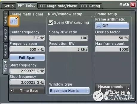
Figure 18 R&S digital oscilloscope spectrum analysis settings
The center frequency is set to 3 GHz, the RBW is set to 5 kHz, and the window function uses a Blackman Harris window. The results of the spectrum analysis are shown in Figure 19. We noticed that due to the DDC structure, the sampling rate is set to 2.5GSa/s, and it is not necessary to satisfy the relationship of the signal frequency more than twice, because the sampling rate at this time is actually the resampling rate in the spectrum analysis. It can be seen from the frequency domain measurement results that the signal frequency is 3 GHz, which is consistent with the output frequency of the signal source. Therefore, it can be seen that using the R&S oscilloscope spectrum analysis structure, even for high frequency signals, still has good frequency resolution.
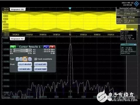
Figure 19 R&S digital oscilloscope spectrum analysis results
Nantong Boxin Electronic Technology Co., Ltd. , https://www.ntbosen.com