FPGA Aviation Bus Protocol Interface Circuit Analysis
The data bus is one of the first digital electronic devices used in aircraft avionics systems. Its typical representative is the internal time division command/response multiplex data bus MIL-STD-1553B. It uses a shielded twisted pair for data transmission with clock information. High reliability 1553B has become a military bus standard widely used in China's aerospace industry. Since the 1553B bus protocol controller basically relies on imported dedicated devices, it is expensive and limited, and these devices require peripheral hardware circuits to work together. If the entire bus interface board is designed, a separate MCU is required, and the integration is not High, which limits the design ability to some extent. With the development of embedded technology, programmable system-on-chip design SoPC technology has been widely used in many fields. SoPC technology is adopted here, and the Virtex-II Pro FPGA is taken as the core to realize the interface logic design of the 1553B air bus transmission protocol.
1553B Airbus Transmission Protocol Standard
The widely adopted 1553B standard is based on the 1973 Army Standard 1553 original. The 1553B is a centralized control, aircraft internal time division command/response multi-channel serial data bus standard. High reliability and flexibility. It has become a key technology for the interconnection of modern airborne system equipment. Widely used in aircraft, ships and other weapons platforms. The 1553B data bus has a transfer rate of 1 Mb/s. The protocol specifies three words: command word, data word, and status word. The word is 20 bits long and consists of a sync header (3 bit) message block (16 bit) and a parity bit (1 bit). The maximum amount of information is 32. The bus system consists of a bus controller (BC) with no more than 31 remote terminals (RT), and sometimes a bus monitor (MT) can be added to the system. The information formats transmitted on the bus mainly include BC to RT, RT to BC, RT to RT, and broadcast mode and system control mode.
system design
The system is based on Xilinx's Virtex-II Pm XC2VP30 FPGA, which features two PowerPC 405 processor cores. The bus interface protocol implementation is based on the Xilinx Virtex-II Pro development system platform, and the Virtex-II Pro development platform is the core of the entire system. This can quickly build a 1553B bus implementation platform. The hardware platform of the system is mainly composed of Vinex-II Pro development board, bus converter, bus terminal equipment and main control computer. The system structure is shown in Figure 1.
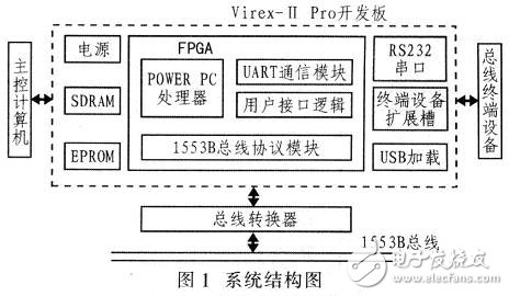
In the system development, in order to improve the development efficiency, the system mainly verifies the 1553B bus protocol module, so the Xilinx Virtex-II Pro development board can be fully utilized. The development board has a wealth of resources, including: XC2VP30 device, SDRAM (expandable to 2 GB), high-speed SelectMAPFPGA configuration PROM, RS232 serial port, USB configuration port embedded in the platform, high-speed system expansion interface (I/O with FPGA) The feet are connected) and can be selected in differential or single-ended mode, PS2 interface, AC97 audio interface, on-board 10/100 M Ethernet device, and so on. These rich on-board resources support the development of 1553B bus protocol logic.
The development of the 1553B bus protocol is mainly developed in FPGA devices, so the performance of the FPGA itself will affect the development of the system. The XC2VP30 has 2 PowerPC 405 processor cores, 13 969 Slices, 428 KB of distributed RAM, 136 multiplier units, 2 448 KB of block RAM, 8 DCMs, and 8 multi-gigabit transceivers. Therefore, the XC2VP30 FPGA is chosen to fully meet the 1553B bus logic development requirements.
The system is designed using the Virtex-II Pro Series XC12VP30 FPGA, and FPGA configuration is a critical issue in hardware design. The FPGA configuration is to program its contents. FPGAs using the SRAM process need to be reconfigured each time they are powered up. The XC2VP30 selects the configuration mode by mode pin, where M2, M1 and M0 are dedicated pins, and HSWAP_EN is combined with the configuration mode pin to determine whether the I/O pin has a pull-up function during configuration. By default, HSWAP_EN is set high, which turns off the pull-up function of the I/O pin during configuration; when it is asserted low, the I/O pin has a pull-up function. When certain configuration modes are selected, CCLK can be used as the signal output pin of the FPGA or as an input signal to the external clock. These pins are not affected by VCCO, but use a 2.5 V auxiliary power supply (VCCAUX).
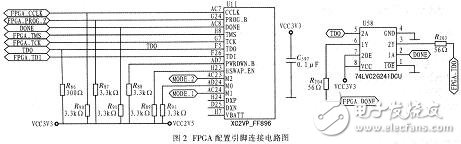
Figure 2 shows the FPGA configuration pin connection circuit diagram. The XC2VP30 supports five configuration modes: Slave-serial mode, Master-serial mode, Slave SelectMAP mode, MasterSelectMAP mode, and Boundary-Scan (IEEE 1532/IEEE 1149) mode. Adjust the configuration mode by adjusting the configuration pins MO, M1, M2. The system design only provides two configuration modes. In the XC2VP30 configuration circuit, the M0 pin is pulled high, so only the MasterSelectMAP mode and the Boundary-Scan mode (ie, boundary scan mode) can be selected. The Master SelectMAP mode is the main version mode of the SelectMAP mode. Under the action of the CCLK signal provided by the XC2VP30, the device configures the [X7:D0] of the device XCF32P through the byte-wide data bus, except that the CCLK is provided by the FPGA. The configuration timing is similar to the Slave SelectMAP mode. In boundary scan mode, the XC2VP30 is configured according to the IEEE 1149.1 standard through dedicated configuration pins CCLK, DONE, PROG_B, TDI, TDO, MS, and TCK.
The SoPC-based design method was used to complete the development of the MIL-STD-1553B aviation bus interface logic and to utilize the instrument test system. The bus protocol interface logic of the system design is solidified into the FPGA. It can replace the special 1553B bus controller device imported from abroad, so as to get rid of the long-term dependence on foreign imported devices, it has good military and economic benefits. The innovation of this system is to develop FPGA with advanced SoPC technology, fully realize 1553B bus interface logic, the system has flexible configuration and easy to expand.
Pro Audio Speaker,18 Woofer Speaker,Subwoofer Loudspeaker,18 Inch Woofer Speaker
Guangzhou Yuehang Audio Technology Co., Ltd , https://www.yhspeakers.com